SLVUBN2 May   2022 TPS62088A , TPS62089A


  1. 1Introduction
    1. 1.1 Performance Specification
    2. 1.2 Modifications
      1. 1.2.1 Fixed Output Voltage Operation
      2. 1.2.2 Input and Output Capacitors
  2. 2Setup
    1. 2.1 Input and Output Connector Descriptions
    2. 2.2 Setup
  3. 3Board Layout
  4. 4Schematic and Bill of Materials
    1. 4.1 Schematic
    2. 4.2 Bill of Materials

Board Layout

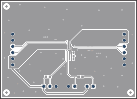
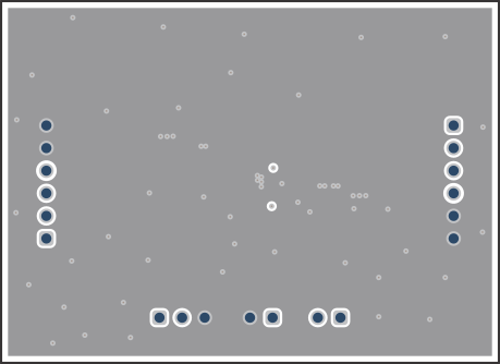
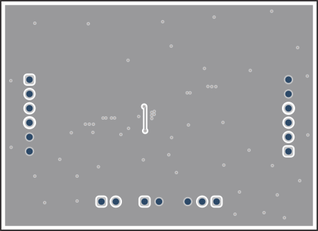
This section provides the TPS6208xEVM-187 board layout and illustrations in Figure 3-1 through Figure 3-5. The Gerbers are available on the TPS6208xEVM-187 EVM product page.
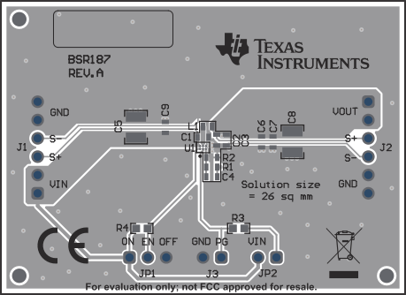
GUID-20220422-SS0I-PR44-VDDG-HMTH2FNRW82H-low.gif Figure 3-1 Top Assembly
GUID-20220422-SS0I-MS85-PV2S-S6XCQGLLPKWS-low.gif Figure 3-2 Top Layer
GUID-20220422-SS0I-HJJS-Z0PD-H1Z5FVRQ8VRJ-low.gif Figure 3-3 Signal Layer 1
GUID-20220422-SS0I-GNGR-FSXB-ZXJ23BHRNVDX-low.gif Figure 3-4 Signal Layer 2
GUID-20220422-SS0I-LJMQ-HSJC-5F4JHHQDJVXB-low.gif Figure 3-5 Bottom Layer