SLVUBO3A April 2019 – October 2020 TPS650330-Q1
- Trademarks
- 1BOOSTXL-TPS65033 Components and Environment
- 2BOOSTXL-TPS65033 Board Information
- 3Programming GUI Operation
- 4Recommended Operating Procedure
- 5BOOSTXL-TPS65033 Schematic
- 6BOOSTXL-TPS65033 Board Layers
- 7BOOSTXL-TPS65033 Bill of Materials
- 8Revision History
2 BOOSTXL-TPS65033 Board Information
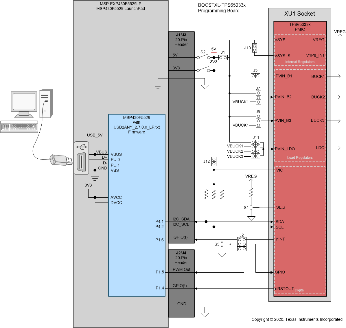
The BOOSTXL-TPS65033 is designed to stack on top of a LaunchPad, connecting the relevant power and MCU pins to the PMIC through the headers J1/J3 and J2/J4. Power is delivered to the PMIC from the USB port of a PC through the the LaunchPad 5 V and 3.3 V rails. The following block diagram demonstrates how the LaunchPad interfaces with the PC and the PMIC.
 Figure 2-1 Programming Board and LaunchPad
Connections