SLVUBU4 March 2021
- Trademarks
- 1Introduction
-
2Description
- 2.1 Input Power and Load (J1/J3 and J2/J4):
- 2.2 Enable Control (J5):
- 2.3 Over Voltage Protection (J6):
- 2.4 Two Back-Back Connected MOSFETs (Q1/Q3 and Q2):
- 2.5 Output Slew Rate Control (R2 and C4):
- 2.6 Output Schottky Diode (D3) and LED Indication:
- 2.7 TVS Selection for 200-V Unsuppressed Load Dump Protection:
- 2.8 Test Points:
- 3Schematic
- 4Test Equipment Requirements
- 5Test Setup and Results
- 6Board Layout and Bill of Materials
- Revision History
6.1 Board Layout
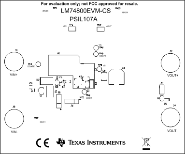
 Figure 6-1 Component Placement
TOP
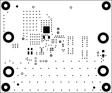
 Figure 6-2 Component Placement
BOTTOM
 Figure 6-3 TOP Layer Routing
 Figure 6-4 BOTTOM Layer Routing