SLVUBU6A April 2020 – June 2020 TPS274160
4 TPS274160 EVM Assembly Drawings and Layout
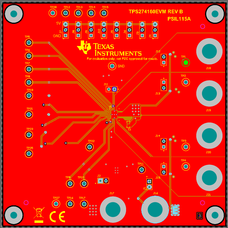
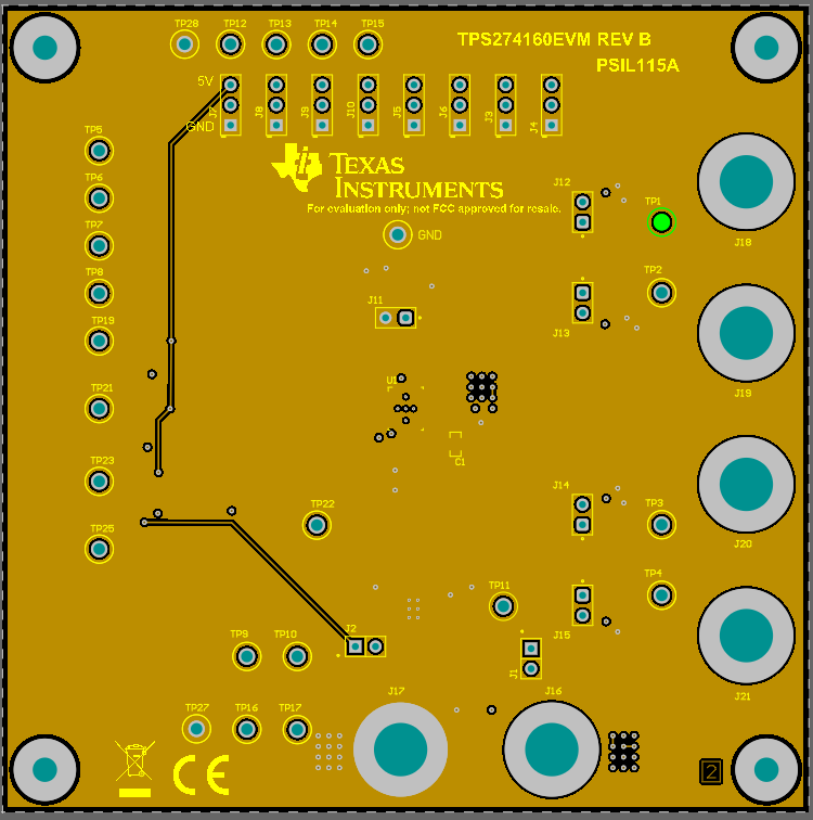
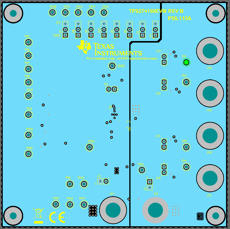
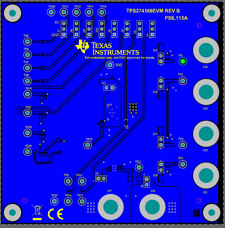
Figure 2 to Figure 5 show the design of the TPS274160 printed-circuit board (PCB). The EVM is designed using FR4 material, four-layer (2s2p), 2 × 70-µm Cu in top and bottom layers, and 2 × 35-µm Cu in internal plane layers. All components are in an active area on the top side and all active traces to the top and bottom layers to allow the user to easily view, probe, and evaluate. Moving components to both sides of the PCB offers additional size reduction for space-constrained systems.
 Figure 2. TPS274160EVM First Layer (Top View)
  Figure 3. TPS274160EVM Second Layer GND (Top View)
  Figure 4. TPS274160EVM Third Layer Power Split (Top View)
  Figure 5. TPS274160EVM Bottom Layer (Top View)