SLVUBW7 May   2020


  1.   TPS7H4001QEVM-CVAL Evaluation Module User's Guide
    1.     Trademarks
    2. 1 TPS7H4001QEVM-CVAL Overview
      1. 1.1 Features
      2. 1.2 Applications
    3. 2 TPS7H4001QEVM-CVAL Default Configuration
    4. 3 TPS7H4001QEVM-CVAL Initial Setup
    5. 4 TPS7H4001QEVM-CVAL Testing
      1. 4.1 Output Voltage Regulation
      2. 4.2 Quadrature Phases
      3. 4.3 Output Voltage Ripple
      4. 4.4 Soft Startup
      5. 4.5 Transient Response to Positive/Negative Load Step (27 A to 67 A to 27 A)
      6. 4.6 Loop Frequency Response
      7. 4.7 Efficiency
      8. 4.8 Current Limiting
      9. 4.9 Current Sharing
    6. 5 TPS7H4001QEVM-CVAL EVM Schematic
    7. 6 TPS7H4001QEVM-CVAL Bill of Materials (BOM)
    8. 7 Board Layout
    9. 8 Appendix A

Board Layout

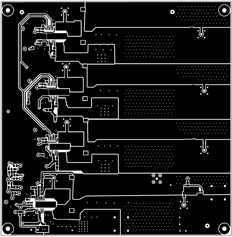
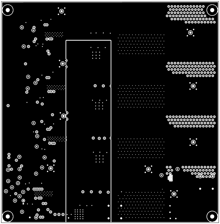
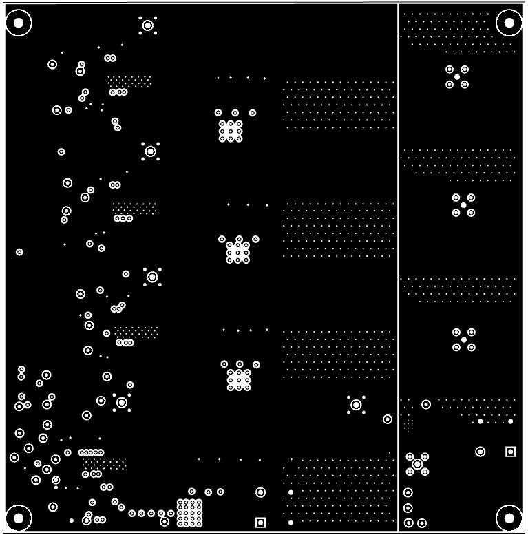
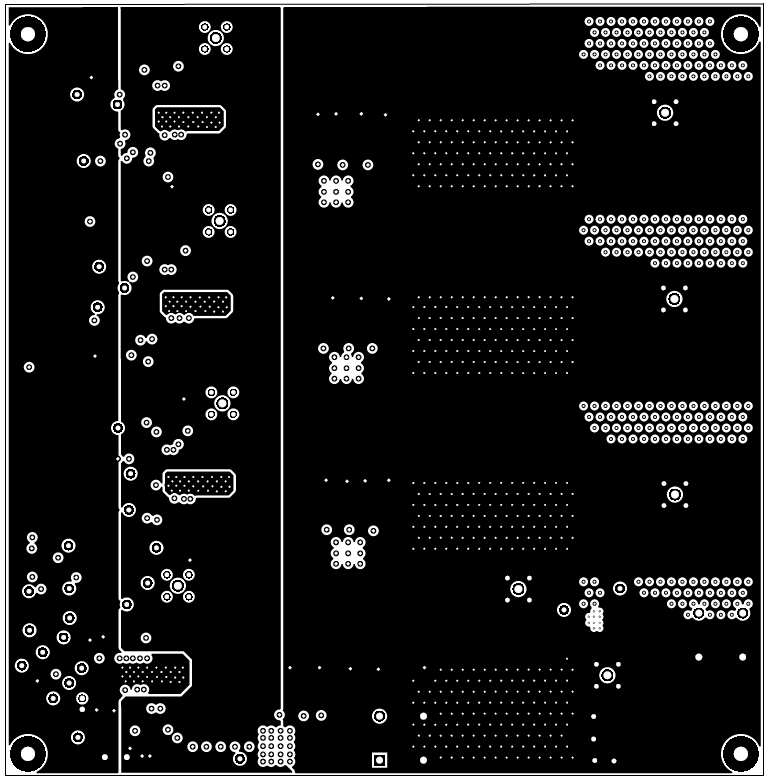
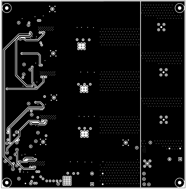
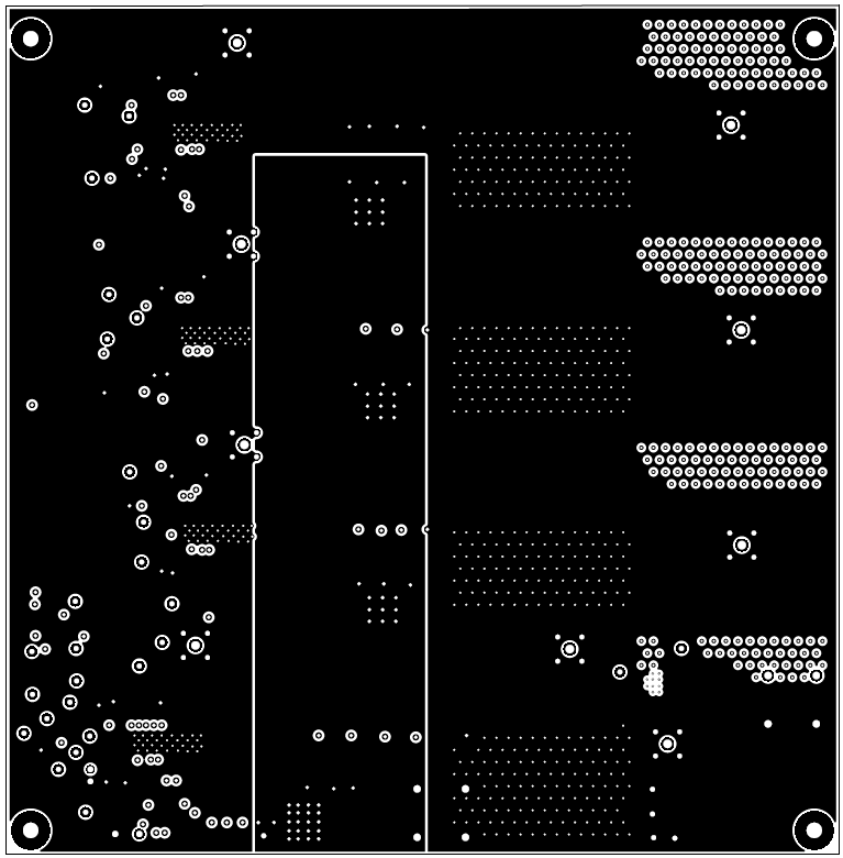
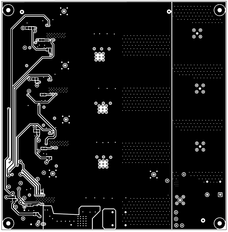
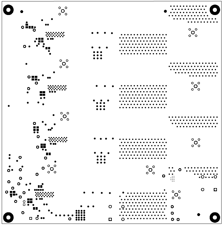
The following is the layer stack of the TPS7H4001QEVM-CVAL board.
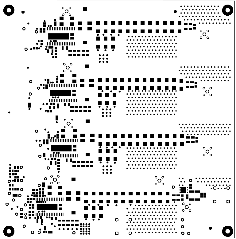
TPS7H4001QEVM-CVAL 015_TOP_OVERLAY.pngFigure 23. Top Overlay
TPS7H4001QEVM-CVAL 016_TOP_SOLDER.pngFigure 24. Top Solder
TPS7H4001QEVM-CVAL 017_TOP_LAYER.pngFigure 25. Top Layer
TPS7H4001QEVM-CVAL 018_SIGNAL_LAYER_ONE.pngFigure 26. Signal Layer One
TPS7H4001QEVM-CVAL 019_SIGNAL_LAYER_TWO.pngFigure 27. Signal Layer Two
TPS7H4001QEVM-CVAL 020_SIGNAL_LAYER_THREE.pngFigure 28. Signal Layer Three
TPS7H4001QEVM-CVAL 021_SIGNAL_LAYER_FOUR.pngFigure 29. Signal Layer Four
TPS7H4001QEVM-CVAL 022_SIGNAL_LAYER_FIVE.pngFigure 30. Signal Layer Five
TPS7H4001QEVM-CVAL 023_SIGNAL_LAYER_SIX.pngFigure 31. Signal Layer Six
TPS7H4001QEVM-CVAL 024_BOTTOM_LAYER.pngFigure 32. Bottom Layer
TPS7H4001QEVM-CVAL 025_BOTTOM_SOLDER.pngFigure 33. Bottom Solder
TPS7H4001QEVM-CVAL 026_BOTTOM_OVERLAY.pngFigure 34. Bottom Overlay