SLVUBX0A July 2021 – January 2022 TPSM8A28 , TPSM8A29
3 Getting Started With the TPSM8A29EVM
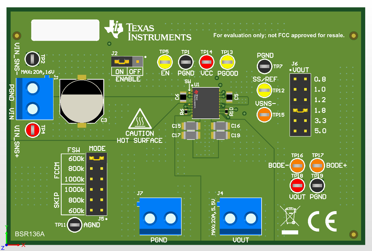
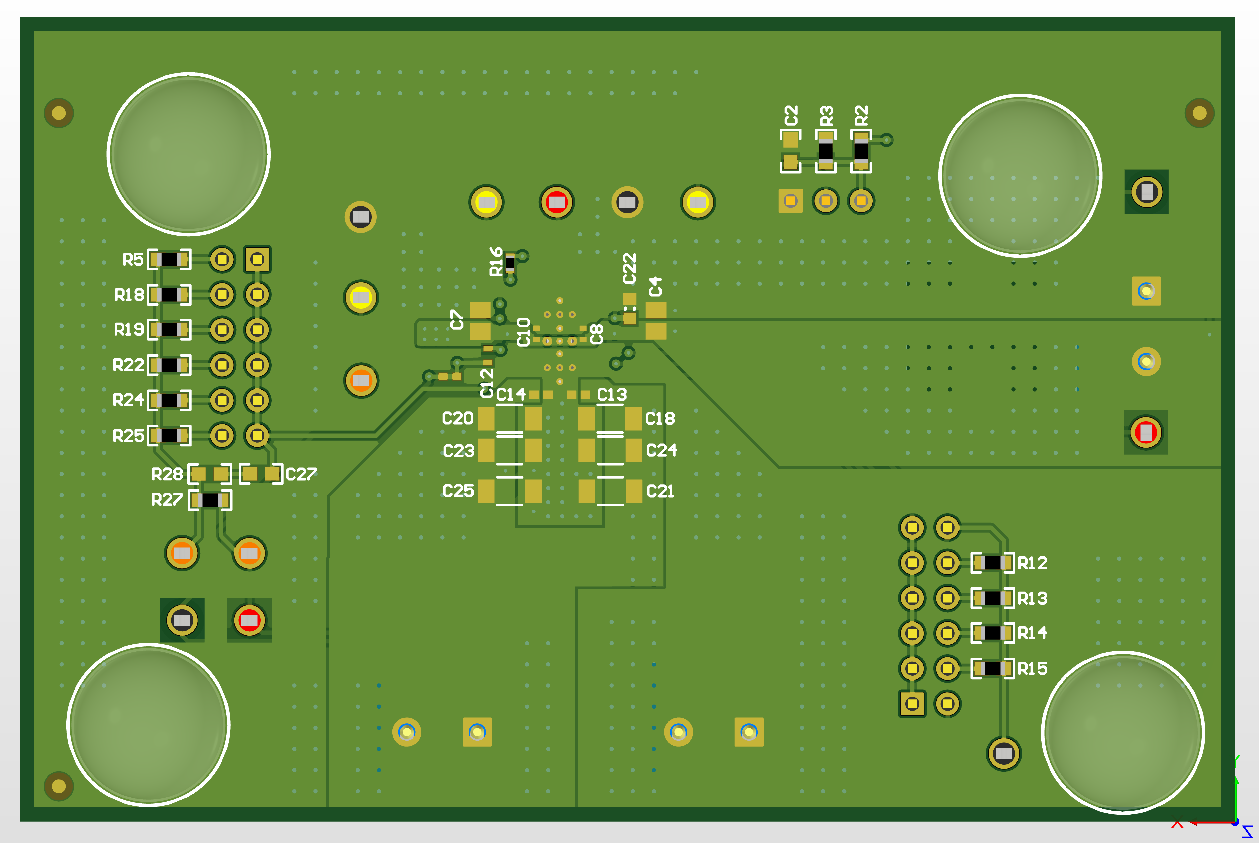
Figure 3-1 and Figure 3-2 show the user interface of the TPSM8A29EVM. A description of the input and output connections is shown in Table 3-1. A description of the headers is shown in Table 3-2 . Further details and considerations are given after the tables.
 Figure 3-1 TPSM8A29EVM 3-D Top View
 Figure 3-2 TPSM8A29EVM 3-D Bottom
View
Figure 3-2 TPSM8A29EVM 3-D Bottom
ViewTable 3-1 Input and Output Connection
Descriptions
| Connector | Description |
|---|---|
| J1 | Positive and negative input voltage supply connection, 4 V - 16 V |
| J4 | Positive output voltage connection, 0.8 V - 5 V |
| J7 | Negative output voltage connection |
Table 3-2 Header Descriptions
| Header | Description |
|---|---|
| J2 | Enable header |
| J5 | Switching frequency and FCCM/DCM operation selection header |
| J6 | Output voltage selection header |