SLVUBX5B August 2023 – February 2024 TPS25762-Q1 , TPS25772-Q1
4.6.3 Thermal Foldback
Thermal foldback related parameters can be configured in this page. Thermal foldback allows the system to reduce power when defined device thermal thresholds are reached, helping to automatically manage power versus temperature system requirements.
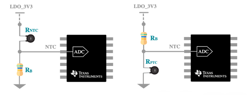
Thermal phase is monitored via the NTC device pin (GPIO5) with a thermistor resistor network as described in Figure 4-2. Only positive voltage slope (from lowest to highest temperature) is supported with NTC or PTC thermistor configurations.
 Figure 4-2 Thermistor Implementation Options: NTC and PTC
Circuit Diagrams
Figure 4-2 Thermistor Implementation Options: NTC and PTC
Circuit DiagramsPHASE 1 is the first thermal foldback phase followed by PHASE 2 and finally PHASE 3. Voltage thresholds must be configured from lowest to highest temperature starting from PHASE 1. Input voltage levels can be calculated based upon the type of thermistor and external resistor values used in the target system hardware design. See the thermistor data sheet for voltage input calculations applicable for each phase as required for the given application operation. When enabled in the GUI, one of two provided preset values can be selected:
PRESET1 is based upon an NTC with RB = 3 kΩ and RNTC = 47 kΩ.
| Voltage Threshold | Voltage/Temp |
|---|---|
| Phase 1 VTHF | 0.392 V (40°C) |
| Phase 1 VTHR | 0.574 V (50°C) |
| Phase 2 VTHF | 0.686 V (55°C) |
| Phase 2 VTHR | 0.938 V (65°C) |
| Phase 3 VTHF | 1.078 V (70°C) |
| Phase 3 VTHR | 1.386 V (80°C) |
PRESET2 is based upon a PTC (TMP61) with RB = 10 kΩ.
| Voltage Threshold | Voltage/Temp |
|---|---|
| Phase 1 VTHF | 1.82 V (40°C) |
| Phase 1 VTHR | 1.876 V (50°C) |
| Phase 2 VTHF | 1.904 V (55°C) |
| Phase 2 VTHR | 1.96 V (65°C) |
| Phase 3 VTHF | 1.988 V (70°C) |
| Phase 3 VTHR | 2.03 V (80°C) |
The CUSTOM option is available to allow up to 6 PHASES and for user-defined setpoints based on voltage and temperature relationships for other thermistor resistor network designs.
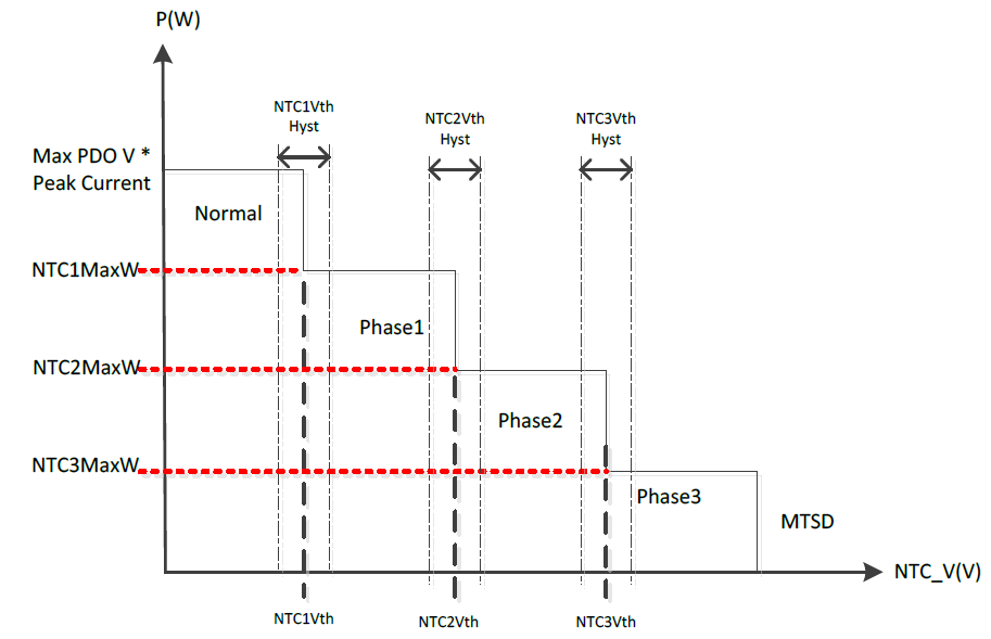
 Figure 4-3 Thermal Foldback Phase vs Maximum Port
Power
Figure 4-3 Thermal Foldback Phase vs Maximum Port
PowerMaximum power for each phase is a configurable total port power output for each thermal foldback phase. Program the maximum power relative to the total VBUS power. Note that if maximum power for a given thermal foldback phase is less than the user-defined total minimum port power (sum of minimum port power in dual port systems), the ports are disabled upon entry into the corresponding thermal foldback phase.
Dual port example:
- Total USB VBUS Power = 100 W
- VBUS Port A maximum power = 60 W and VBUS Port B maximum power = 60 W
- VBUS Port A minimum power = 15 W and VBUS Port B minimum power = 15 W
- Maximum power for PHASE1 = 60 W
- Once this phase is entered, the total USB VBUS power is reduced to 60 W total for ALL ports
-
Maximum power for PHASE2 = 30 W
- Once this phase is entered, total USB VBUS power is reduced to 30 W total for ALL ports
-
Maximum power for PHASE3 = 15 W
- Once this phase is entered, the total USB VBUS power is reduced to 15 W total for ALL ports which is less than the sum of the minimum power of each port (15 W + 15 W = 30 W). In this scenario, the maximum foldback power configured can meet the minimum 15-W requirement of a single port resulting in one port being disabled.