SLVUC03 November   2022 TPS25762-Q1 , TPS25772-Q1


  1.   Abstract
  2.   Trademarks
  3. 1About this Manual
  4. 2Information About Cautions and Warnings
  5. 3Items Required for Operation
  6. 4Introduction
  7. 5Setup
    1. 5.1 Switch, Push Button, Connector, and Test Points Descriptions
    2. 5.2 Jumper Configuration
  8. 6Schematics
    1. 6.1 Main Schematic
    2. 6.2 Sub Schematic – Input Circuit
    3. 6.3 Sub Schematic – Auxiliary Power
    4. 6.4 Sub Schematic – I2C Peripherals
    5. 6.5 Sub Schematic – TPS55288-Q1
    6. 6.6 Sub Schematic – HUB
    7. 6.7 Sub Schematic – TIVA
    8. 6.8 Sub Schematic – ESD
  9. 7 Board Views and Layout Prints
  10. 8Bill of Materials

Main Schematic

Figure 6-1 shows the main schematic of TPS25762EVM-146, Figure 6-2 shows the main schematic of TPS25772Q1EVM-149,and Figure 6-3 shows the main schematic of TPS25772Q1EVM-150.
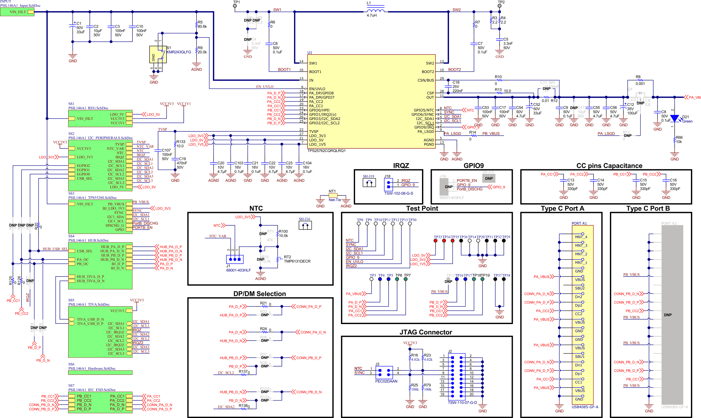
GUID-20221104-SS0I-NHZC-XSRF-KNVXVHD0117X-low.gifFigure 6-1 TPS25762Q1EVM-146 Main Schematic
Figure 6-2 TPS25772Q1EVM-149 Main Schematic
Figure 6-3 TPS25772Q1EVM-150 Main Schematic