SLVUC06 October 2020 TPS650320-Q1
- Trademarks
- 1Introduction
- 2EVM Configurations
- 3Test Points
- 4Graphical User Interface
- 5Typical Performance Plots
- 6TPS650320-Q1 EVM Schematic
- 7TPS650320-Q1 EVM PCB Layers
- 8TPS650320-Q1 EVM Bill of Materials
3.1 Voltage Test Points
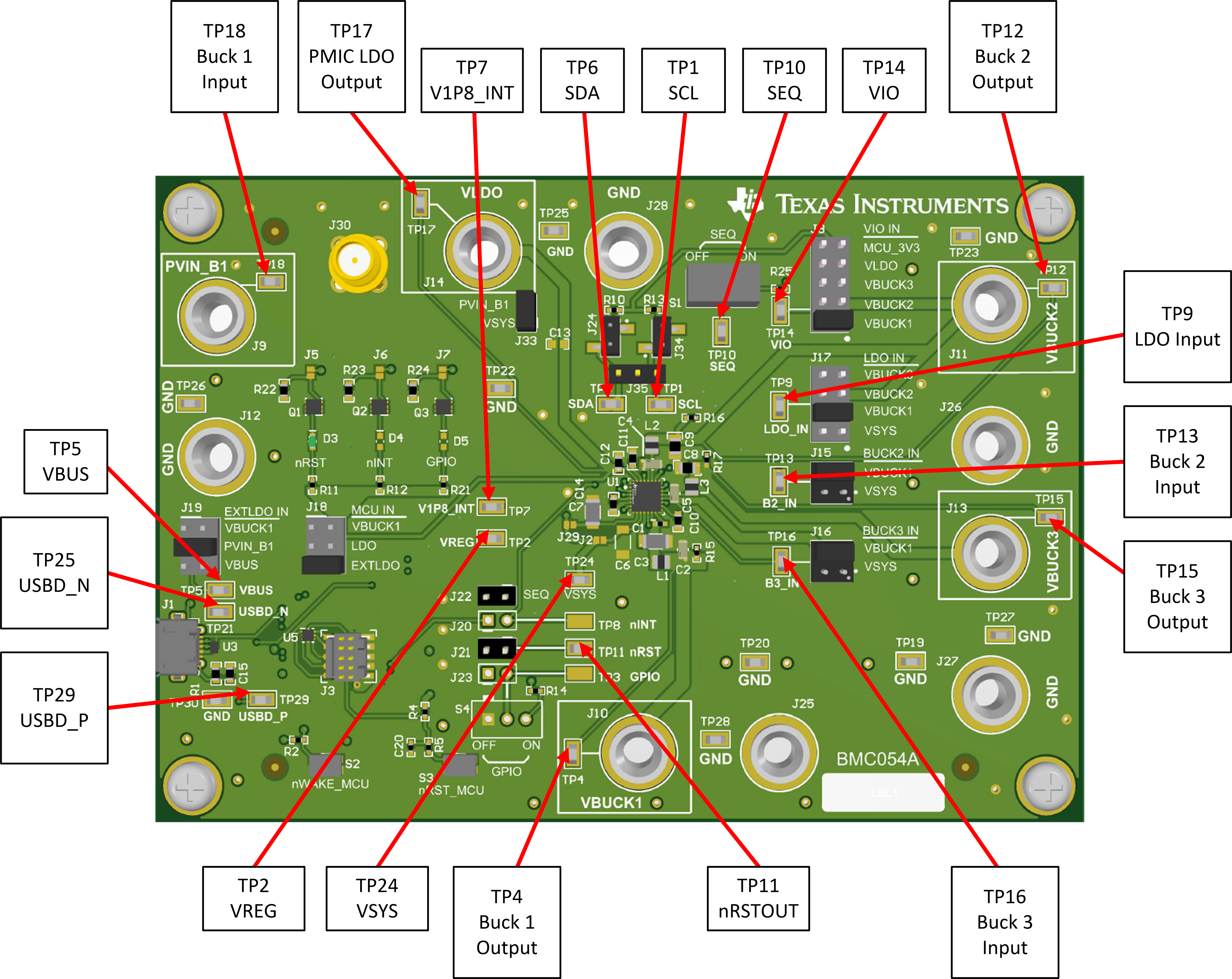
The TPS650320-Q1 EVM contains 30 test points for various measurements. Trace assignments to the test points are shown in Table 3-1. For reference, Figure 3-1 demonstrates the test point locations on the EVM.
Table 3-1 TPS650320-Q1 EVM Test Points
| Test Point Number | Associated Trace |
|---|---|
| TP1 | SCL |
| TP2 | VREG |
| TP4 | Buck 1 Output |
| TP5 | VBUS |
| TP6 | SDA |
| TP7 | V1P8_INT |
| TP9 | PMIC LDO Input |
| TP10 | SEQ |
| TP11 | nRSTOUT |
| TP12 | Buck 2 Output |
| TP13 | Buck 2 Input |
| TP14 | VIO |
TP15 | Buck 3 Output |
| TP16 | Buck 3 Input |
| TP17 | PMIC LDO Output |
| TP18 | Buck 1 Input |
| TP19 | GND |
| TP20 | GND |
| TP21 | USBD_N |
| TP22 | GND |
| TP23 | GND |
| TP24 | VSYS |
| TP25 | GND |
| TP26 | GND |
| TP27 | GND |
| TP28 | GND |
| TP29 | USBD_P |
| TP30 | GND |
 Figure 3-1 TPS650320-Q1 EVM Test Point Locations