SLVUC09 September 2021
3.1 Layout
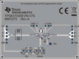
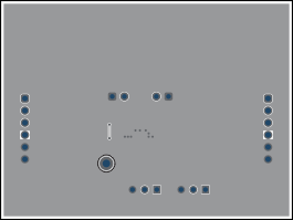
Figure 3-1 and Figure 3-2 show the board layout for the TPS631000EVM-075 PCB.
 Figure 3-1 Top Layer Routing
 Figure 3-2 Bottom Layer Routing
SLVUC09 September 2021
Figure 3-1 and Figure 3-2 show the board layout for the TPS631000EVM-075 PCB.
 Figure 3-1 Top Layer Routing
 Figure 3-2 Bottom Layer Routing