SLVUC10 March   2021 TPS62816-Q1


  1.   Trademarks
  2. 1Warning and Caution
  3. 2Introduction
    1. 2.1 Performance Specification
    2. 2.2 Modifications
      1. 2.2.1 Input and Output Capacitors
      2. 2.2.2 Adjustable-Output IC U1 Operation
      3. 2.2.3 Feedforward Capacitor
      4. 2.2.4 Soft-Start Time
      5. 2.2.5 Tracking
      6. 2.2.6 Switching Frequency and Control Loop Compensation
  4. 3Setup
    1. 3.1 Connector Descriptions
    2. 3.2 Hardware Setup
  5. 4TPS62816EVM-140 Test Results
  6. 5Board Layout
  7. 6Schematic
  8. 7List of Materials

Board Layout

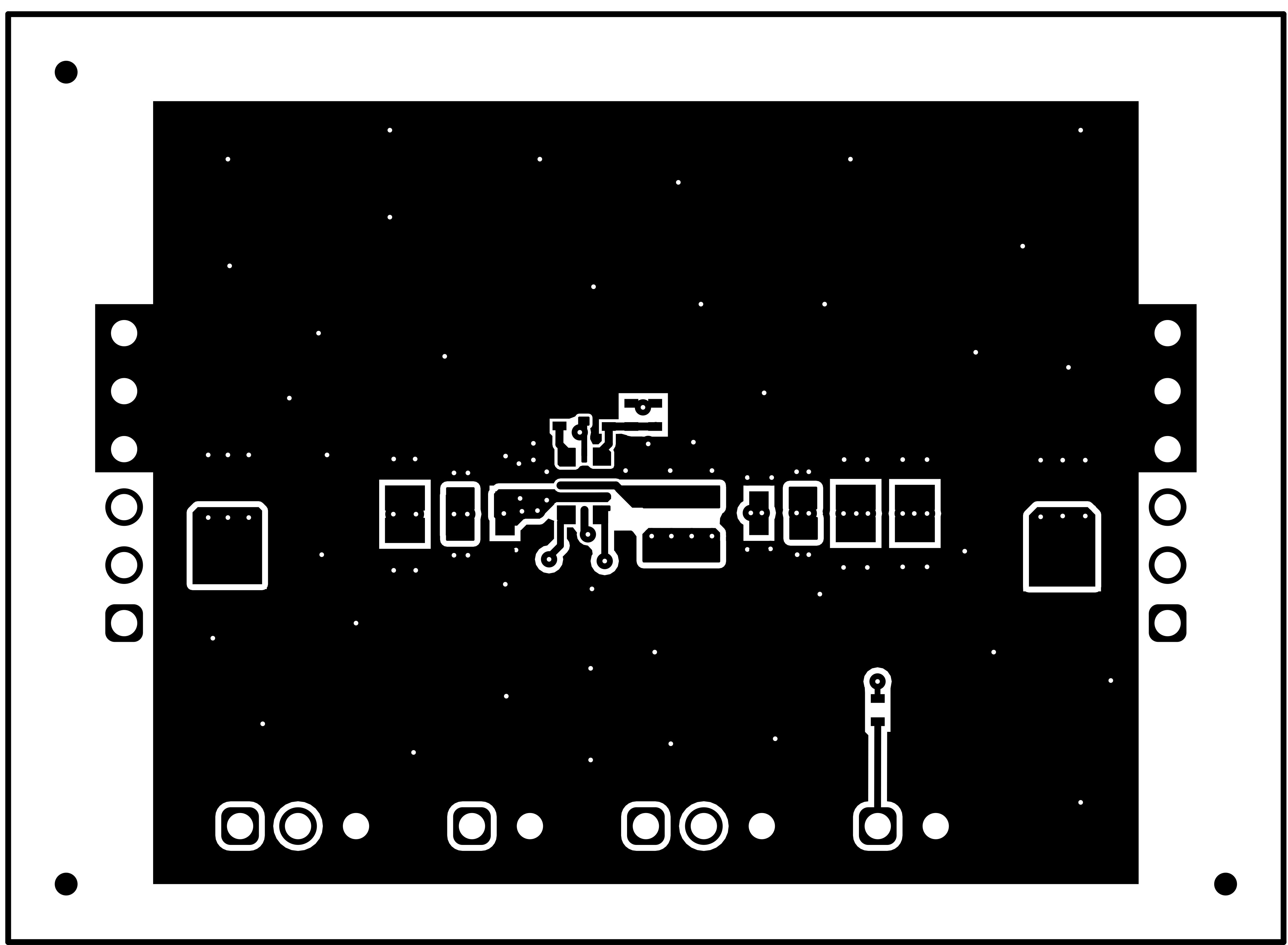
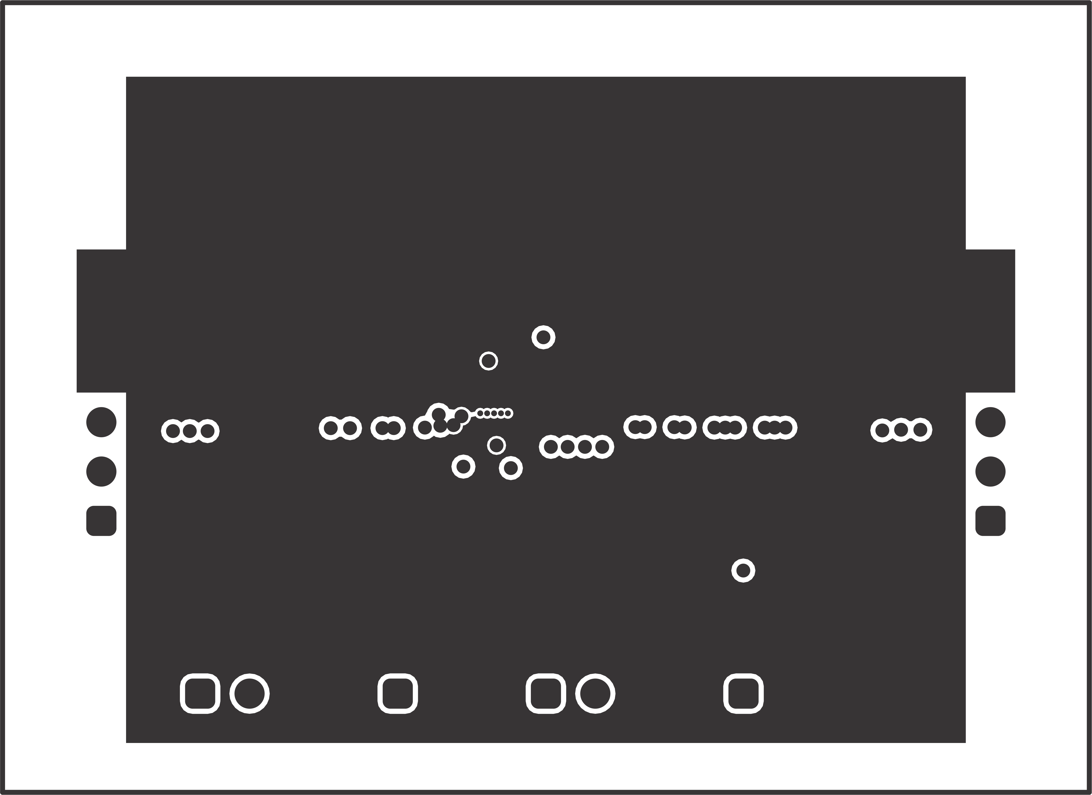
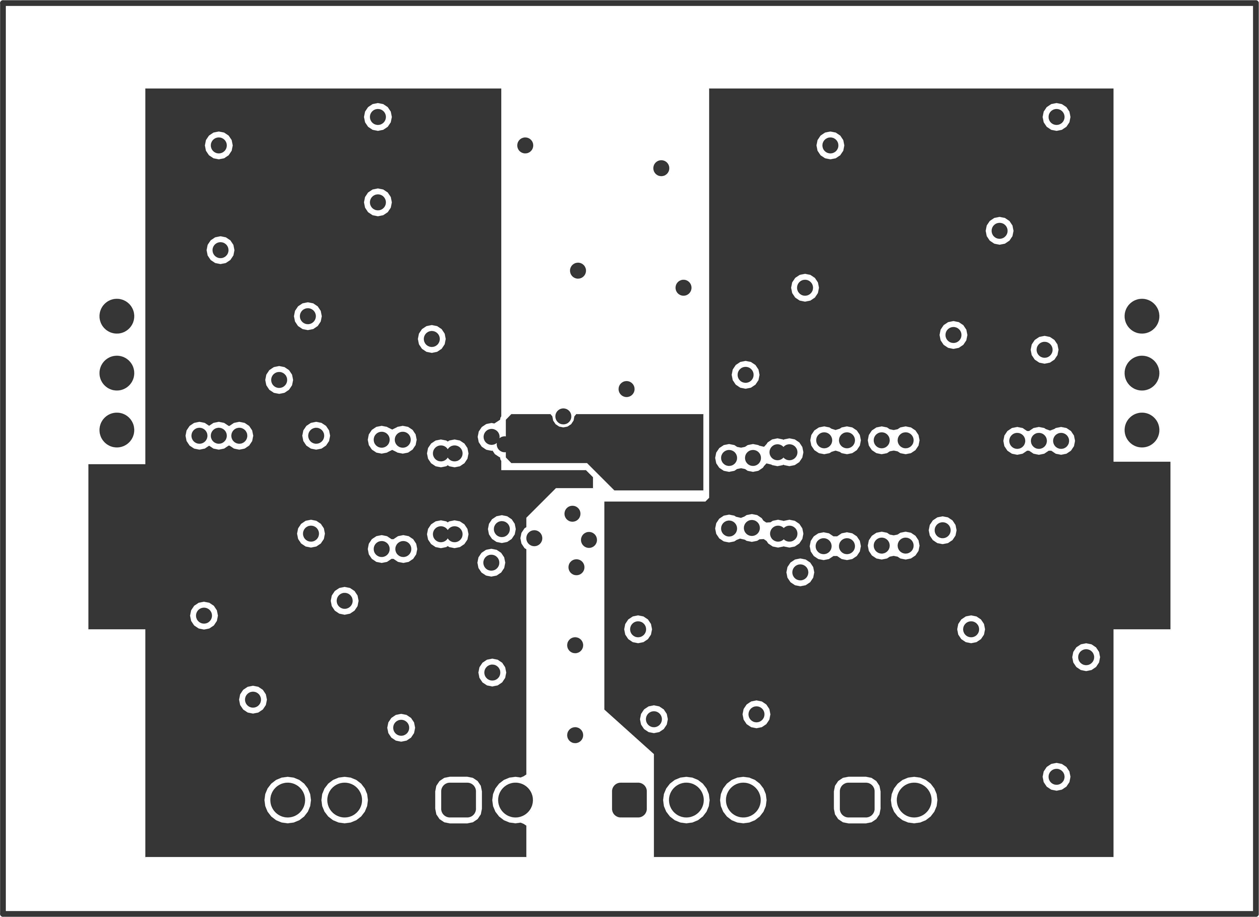
This section provides the TPS62816EVM-140 board layout. The Gerber files are available on the TPS62816EVM-140 tool page

GUID-20201125-CA0I-CNGK-FQKS-M1HKHV7LDD7R-low.gif Figure 5-1 Top Silk
GUID-20201125-CA0I-VQGB-49TM-NVVPT9CDMFBM-low.gif Figure 5-2 Top Layer
GUID-20201125-CA0I-57HB-JG4M-PC1VNQCB5Q2F-low.gif Figure 5-3 Layer 2
GUID-20201125-CA0I-5JB5-H5JC-9B5V0GWRHTPG-low.gif Figure 5-4 Layer 3
GUID-20201125-CA0I-Z74G-S8FR-7DDGCHXBTCVN-low.gif Figure 5-5 Layer 4
GUID-20201125-CA0I-SCJ0-RSNP-Q6VCQKJZH9XT-low.gif Figure 5-6 Layer 5
GUID-20201125-CA0I-LWJH-K942-D1NTHVRKVFQR-low.gif Figure 5-7 Bottom Layer