SLVUC40 May   2021 TPS629210-Q1


  1.   Trademarks
  2. 1Introduction
  3. 2Performance Specification
  4. 3EVM Configuration and Modification
    1. 3.1 Input and Output Capacitors
    2. 3.2 Configurable Enable Threshold Voltage
    3. 3.3 MODE/S-CONF Setting
    4. 3.4 Power Good
    5. 3.5 Power Good Pull Up Voltage
    6. 3.6 Feedforward Capacitor Option
    7. 3.7 Output Voltage Setting
    8. 3.8 Loop Response Measurement
  5. 4EVM Test Set Up
    1. 4.1 Input and Output Connectors
    2. 4.2 Jumper Configuration
      1. 4.2.1 JP1 Enable
      2. 4.2.2 JP2 MODE/S-CONF
      3. 4.2.3 JP3 Power Good
      4. 4.2.4 JP4 PG Pull Up Voltage
  6. 5Test Results
  7. 6Board Layout
  8. 7Schematic and Bill of Materials
    1. 7.1 Schematic
    2. 7.2 Bill of Materials
  9. 8References

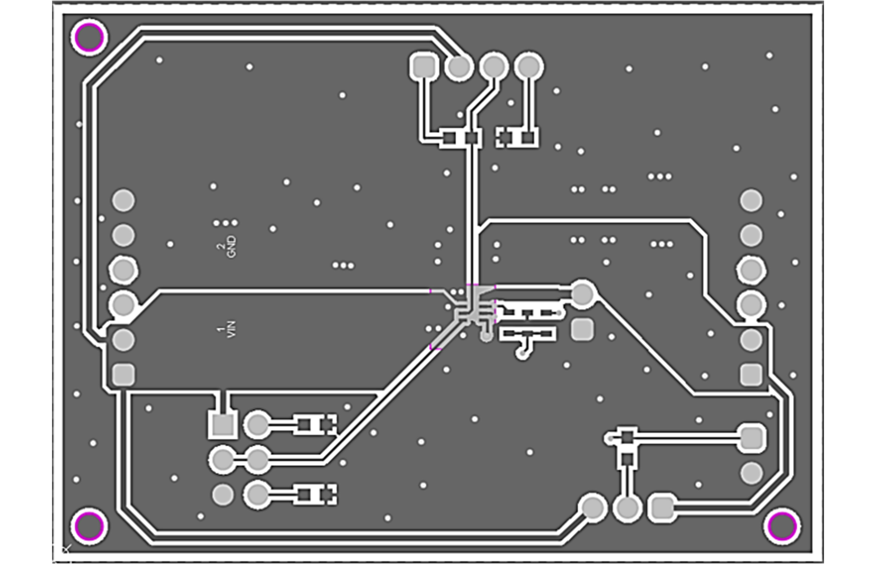
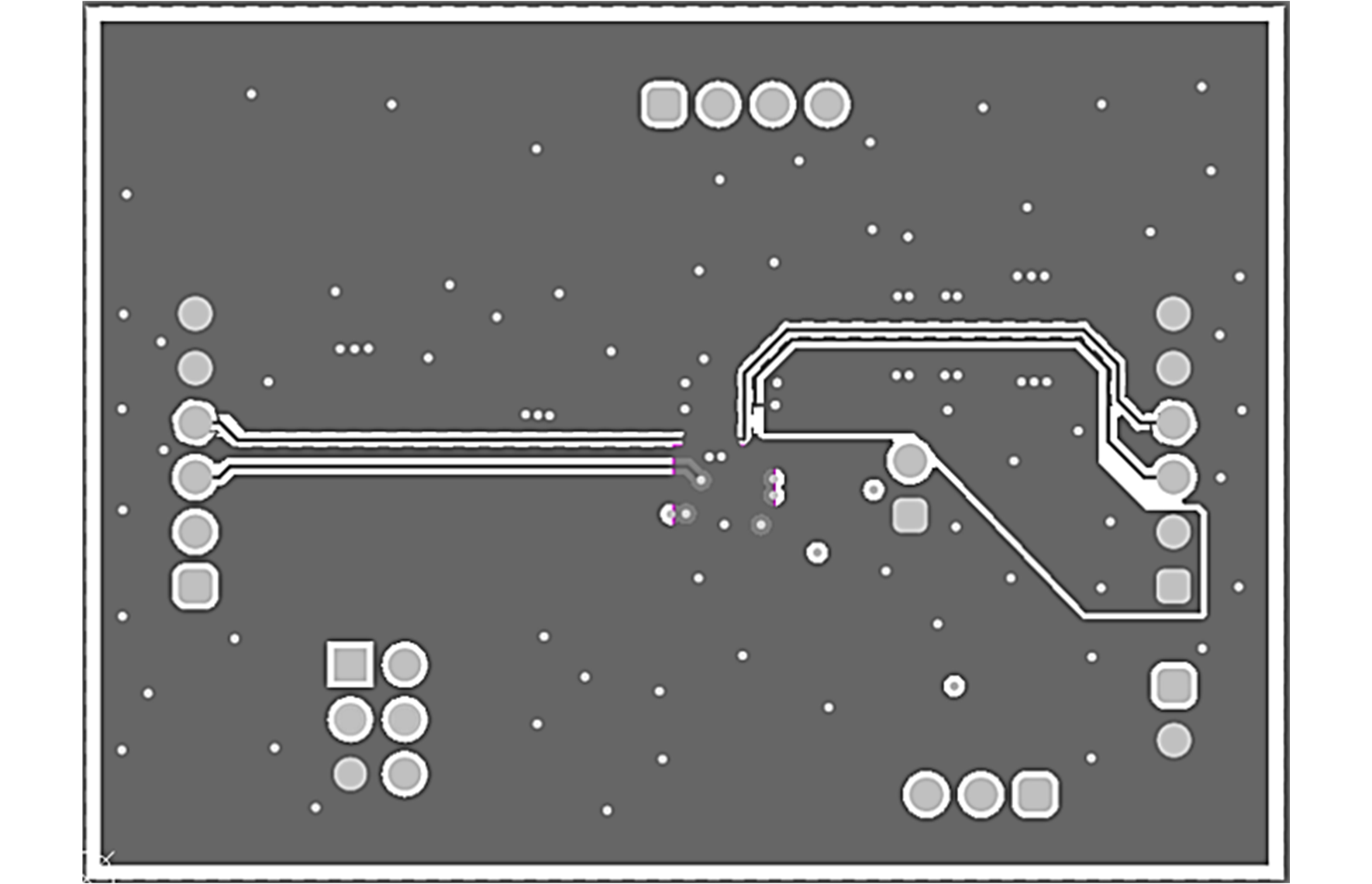
Board Layout

This section provides the EVM board layout and illustrations.
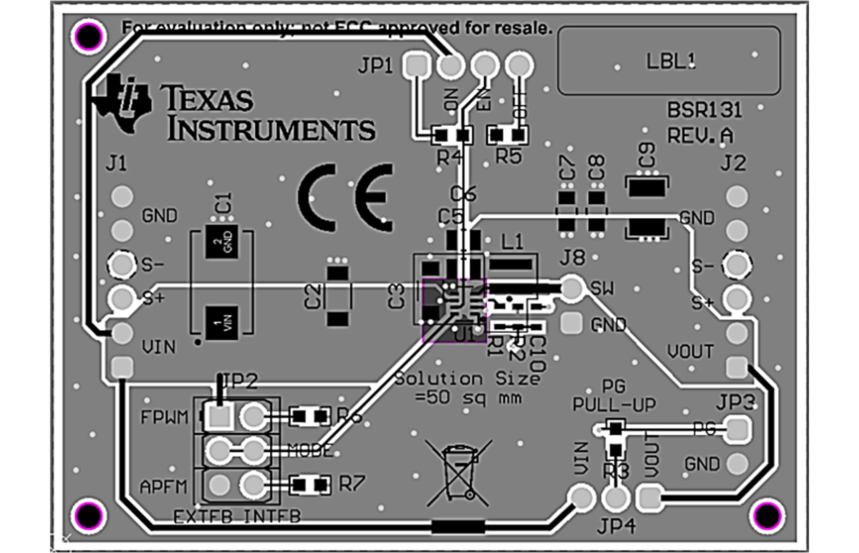
GUID-20210521-CA0I-0JJT-QWMG-GJRJZ0BKJ4HZ-low.png Figure 6-1 Top Assembly
GUID-20210521-CA0I-ZBJ1-JHFQ-1Z87B3X87TJS-low.png Figure 6-2 Top Layer
GUID-20210521-CA0I-CD9L-V5LG-L6QW5TWF6C5B-low.png Figure 6-3 Internal Layer 1
GUID-20210521-CA0I-HZHB-WZXL-HHNLPNJLX8ZM-low.png Figure 6-4 Internal Layer 2
GUID-20210521-CA0I-SWH4-SXW5-DXRZ1TCZXSMF-low.png Figure 6-5 Bottom Layer