-
Using the TPSM5601R5EVM and TPSM5601R5SEVM
Using the TPSM5601R5EVM and TPSM5601R5SEVM
Trademarks
All trademarks are the property of their respective owners.
1 EVM Setup
Figure 1-1 highlights the user interface items associated with the EVM. The VIN Power terminal block (J1) is used for connection to the host input supply and the VOUT Power terminal block (J4) is used for connection to the load. These terminal blocks accept up to 16-AWG wire.
- Use the VIN S+ and VIN S– test points along with the VOUT S+ and VOUT S– test points located near the power terminal blocks as voltage monitoring points where voltmeters can be connected to measure VIN and VOUT. Do not use these S+ and S– monitoring test points as the input supply or output load connection points. The PCB traces connecting to these test points are not designed to support high currents.
- Use the VIN scope (J2) and VOUT scope (J3) test points to monitor VIN and VOUT waveforms with an oscilloscope. These test points are intended to use un-hooded scope probes outfitted with a low inductance ground lead (ground spring) mounted to the scope probe barrel. The two sockets of each test point are on 0.1-in centers. Connect the scope probe tip to the top socket labeled "+" and connect the scope ground lead to the bottom socket.
- The control test points located near the bottom of the EVM test the features of the device. Refer to Section 2 for more information on the individual control test points.
- The VOUT SELECT jumper (J6) is provided to
select the desired output voltage:
- 1.2 V
- 1.8 V
- 2.5 V
- 3.3 V
- 5.0 V
- The device can be turned on or off using the enable jumper (J5). Place the jumper in the ON position to enable the device. Place the jumper in the OFF position to disable the device. The undervoltage lockout (UVLO) can be set by populating resistors R1 and R2 located on the bottom side of the EVM. Refer to the data sheet for recommended UVLO resistor values. The power good (PGOOD) test point is available to monitor when a valid output voltage is present on the EVM. Additionally, the PG_PU pin is present as a convenient point to connect a pullup voltage for the PGOOD signal.
2 EVM Connectors and Test Points
Wire-loop test points and scope probe sockets are included for digital voltmeters (DVM) or oscilloscope probes to aid in the evaluation of the device. Table 2-1(1) describes each test point.
| TEST POINT | DESCRIPTION |
|---|---|
| VIN S+ | Input voltage monitor. Connect the positive lead of a DVM to this point for measuring efficiency. |
| VIN S– | Input ground monitor. Connect the negative lead of a DVM to this point for measuring efficiency. |
| VOUT S+ | Output voltage monitor. Connect the positive lead of a DVM to this point for measuring efficiency, line regulation, and load regulation. |
| VOUT S– | Output ground monitor. Connect the negative lead of a DVM to this point for measuring efficiency, line regulation, and load regulation. |
| PGND | Power ground test points |
| VIN Scope (J2) | Input voltage scope monitor. Connect an oscilloscope probe to this set of points to measure input ripple voltage. |
| VOUT Scope (J3) | Output voltage scope monitor. Connect an oscilloscope probe to this set of points to measure output voltage ripple and transient response. |
| EN (VIN) | Enable test point. EN test point is connected to VIN. Do not connect this test point to ground or any other signal. Use the ENABLE Control header (J5) to disable the device. To monitor the enable signal, monitor pin 2 of header J5. |
| ENABLE Control (J5) | Enable select jumper. Enable or disable the device using a jumper. |
| PGOOD | Power good test point. Monitors the power-good signal of the device. This is an open-drain signal. A 49.9-kΩ resistor is connected to this pin and the PG_PU pin on the EVM. |
| PG_PU | PGOOD pullup test point. Apply a voltage to this pin to use as a pullup voltage for the PGOOD signal. A 49.9-kΩ resistor is connected to this pin and the PGOOD pin on the EVM. |
3 Test Results
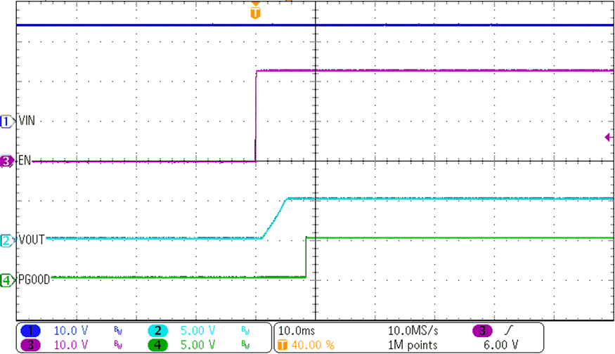
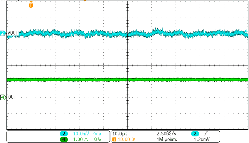
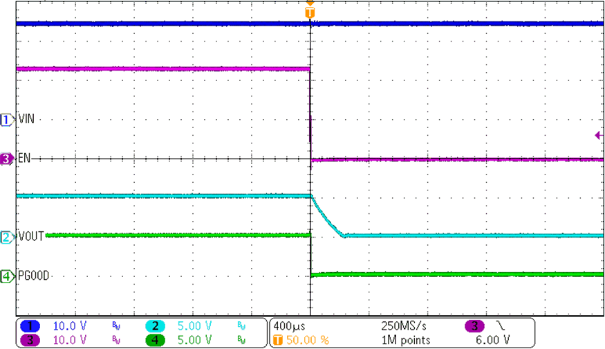
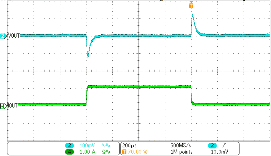
Figure 3-1 through Figure 3-4 demonstrate the performance of the TPSM5601R5EVM under the following condition of a 24-V input voltage, 5-V output voltage, and 1-A load.
 Figure 3-1 ENABLE Start-Up Waveform
 Figure 3-3 Output Voltage
Ripple
 Figure 3-2 ENABLE Shutdown Waveform
 Figure 3-4 Transient
Performance