SLVUCB8A May 2022 – September 2022 TPS25985
- TPS25985 evaluation module for eFuse User's Guide
- Trademarks
- 1Introduction
- 2Description
- 3Schematic
- 4General Configurations
-
5Test Setup and Procedures
- 5.1 Hot Plug
- 5.2 Start-up with Enable
- 5.3 Difference Between Current Limit and DVDT Based Start-up Mechanisms
- 5.4 Power-up into Short
- 5.5 Overvoltage Lockout
- 5.6 Transient Overload Performance
- 5.7 Overcurrent Event
- 5.8 Provision to Apply Load Transient and Overcurrent Event Using an Onboard Switching Circuit
- 5.9 Output Hot Short
- 5.10 PROCHOT# Implementation Using General-Purpose Comparator
- 5.11 Quick Output Discharge (QOD)
- 5.12 Thermal Performance of TPS25985EVM
- 6EVAL Board Assembly Drawings and Layout Guidelines
- 7Bill Of Materials (BOM)
- 8Revision History
6.1 PCB Drawings
Figure 6-1 and Figure 6-2 show the component placements of the EVM. A pictorial representation of the TPS25985EVM PCB layers can be found in Figure 6-3 to Figure 6-10.
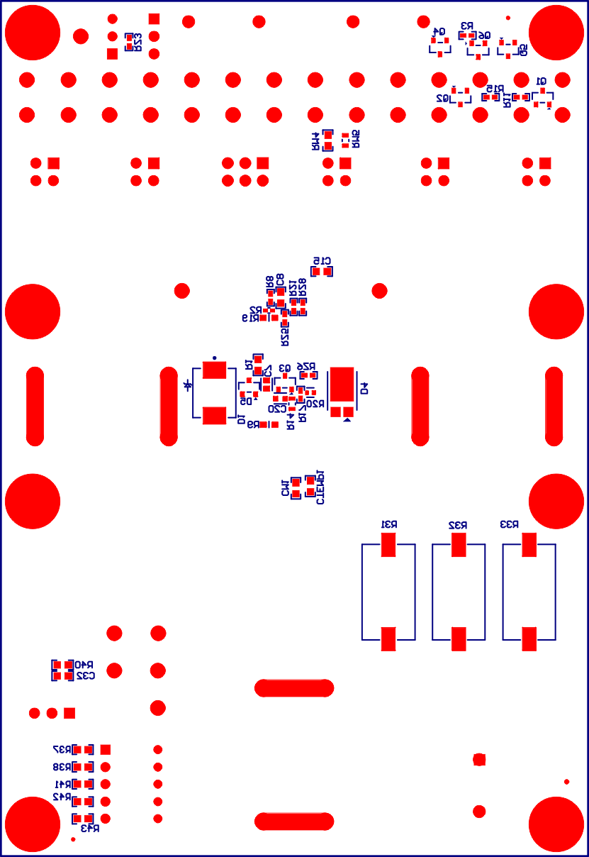 Figure 6-1 TPS25985EVM Board: Top
Assembly
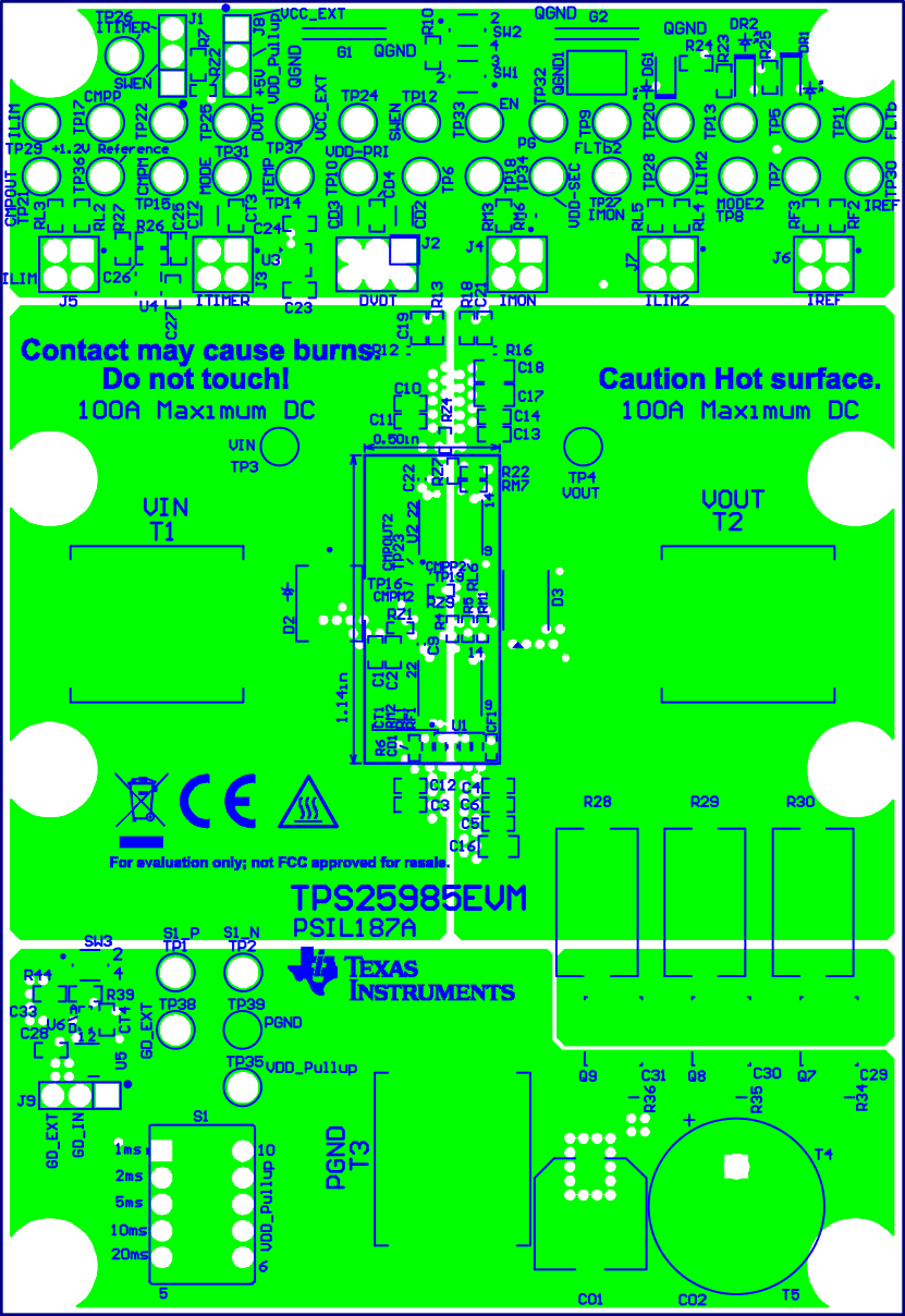 Figure 6-3 TPS25985EVM Board: Top Layer
 Figure 6-5 TPS25985EVM Board: Layer 2
(Power)
 Figure 6-7 TPS25985EVM Board: Layer 4
(Signal)
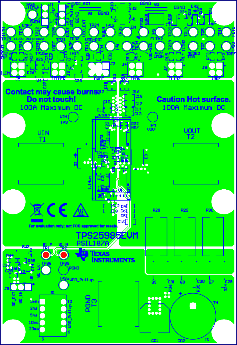 Figure 6-9 TPS25985EVM Board: Layer 6
(Power)
 Figure 6-2 TPS25985EVM Board: Bottom
Assembly
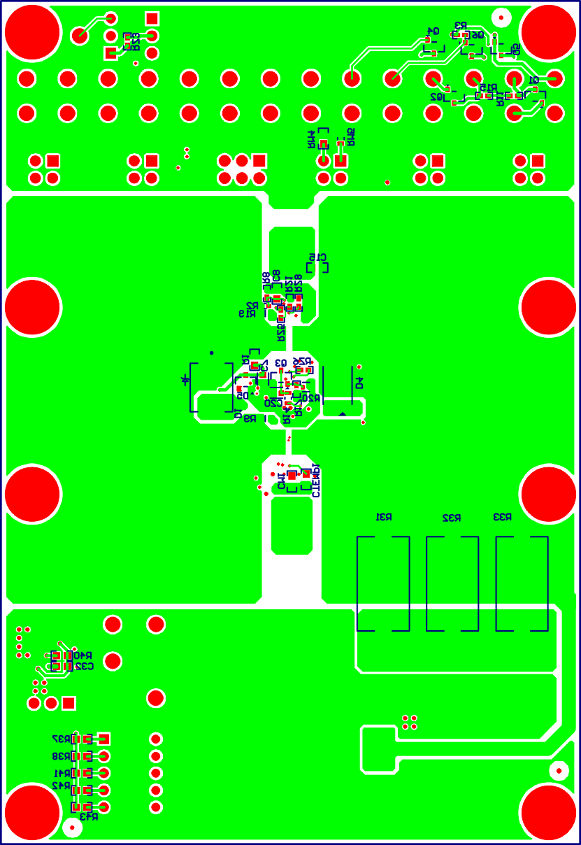 Figure 6-4 TPS25985EVM Board: Bottom
Layer
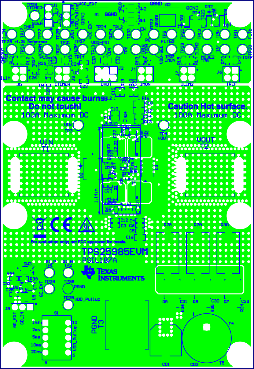 Figure 6-6 TPS25985EVM Board: Layer 3
(Power)
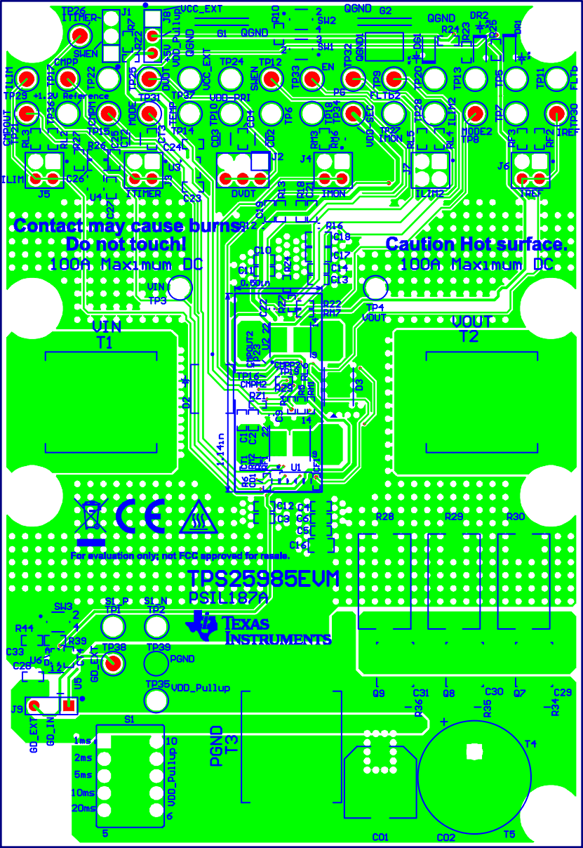 Figure 6-8 TPS25985EVM Board: Layer 5
(Signal)
 Figure 6-10 TPS25985EVM Board: Layer 7
(Power)
Figure 6-10 TPS25985EVM Board: Layer 7
(Power)Note: Analog signal nets, such as IREF, IMON, and
TEMP, should be routed away as much as possible from
power nets, such as VIN, VOUT, and PGND.