SLVUCC0A October   2021  – December 2021 TPS2597


  1.   Trademarks
  2. 1Introduction
    1. 1.1 EVM Features
    2. 1.2 EVM Applications
  3. 2Description
  4. 3Schematic
  5. 4General Configurations
    1. 4.1 Physical Access
    2. 4.2 Test Equipment and Setup
      1. 4.2.1 Power Supplies
      2. 4.2.2 Meters
      3. 4.2.3 Oscilloscope
      4. 4.2.4 Loads
  6. 5Test Setup and Procedures
    1. 5.1 Hot-Plug Test
    2. 5.2 Overcurrent Test
    3. 5.3 Output Hot-Short Test
    4. 5.4 Wakeup into Short Test
    5. 5.5 Overvoltage Clamp Test
  7. 6EVAL Board Assembly Drawings and Layout Guidelines
    1. 6.1 PCB Drawings
  8. 7Bill Of Materials (BoM)
  9. 8Revision History

PCB Drawings

Figure 6-1 shows component placement of the EVAL Board. Figure 6-2 shows PCB layout images.
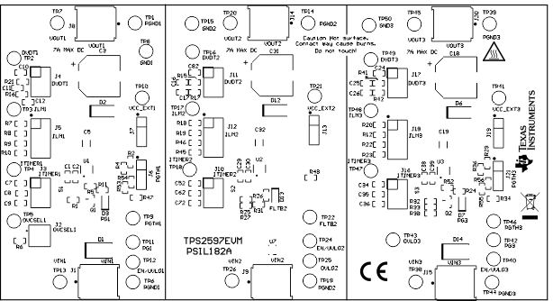
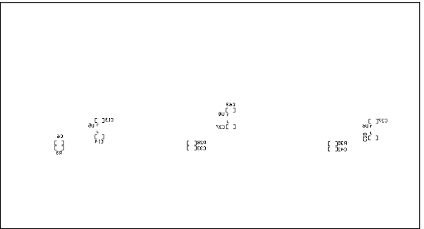
GUID-20211004-SS0I-SW4G-DBXS-MG8VJKRLRTM2-low.gifGUID-20211004-SS0I-6MZT-4PLC-QFRZLXRTPHJH-low.gifFigure 6-1 TPS2597EVM Board (a) Top Assembly (b) Bottom Assembly
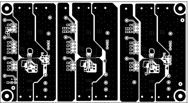
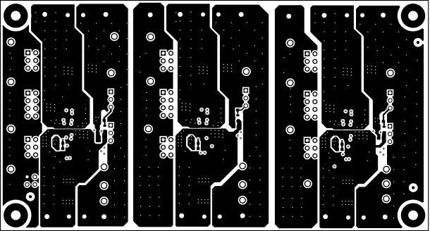
GUID-20211004-SS0I-QQXQ-LCJT-BTNNTLWFNJCS-low.gifGUID-20211004-SS0I-K1P2-CFBM-GRLMMNRJ34MW-low.gifFigure 6-2 TPS2597EVM Board (a) Top Layer (b) Bottom Layer