SLVUCC4 January 2022 TPS629206
3.7 Output Voltage Setting
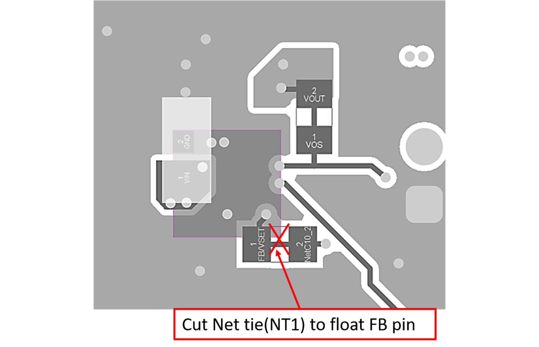
The TPS629206EVM is configured for external feedback as default with an output voltage of 3.3 V set by R1 and R2. Additionally, if the internal feedback (VSET) configuration is used, the user can cut net tie NT1 located on the back of the board (shown in Figure 3-1). This will float the FB pin, resulting in a 3.3-V output voltage using the internal VSET. Resistors R1 and R2 can also be changed to set the output voltage between 0.6 V and 5.5 V. See the TPS629206 data sheet for recommended values. R2 was populated with 34 k so that if the internal (VSET) is chosen while R1 is removed, the device regulates to 1.8-V output voltage.
WARNING: If the output voltage is
increased, ensure the voltage rating of output capacitor C5 is sized appropriately.
 Figure 3-1 Internal Feedback (VSET) Configuration Board
Modification