SLVUCC6 March   2022 TPS629203-Q1


  1.   Trademarks
  2. 1Introduction
  3. 2Performance Specification
  4. 3EVM Configuration and Modification
    1. 3.1 Input and Output Capacitors
    2. 3.2 Configurable Enable Threshold Voltage
    3. 3.3 MODE/S-CONF Setting
    4. 3.4 Power Good
    5. 3.5 Power-Good Pullup Voltage
    6. 3.6 Feedforward Capacitor Option
    7. 3.7 Output Voltage Setting
    8. 3.8 Loop Response Measurement
  5. 4EVM Test Setup
    1. 4.1 Input and Output Connectors
    2. 4.2 Jumper Configuration
      1. 4.2.1 JP1 Enable
      2. 4.2.2 JP2 MODE/S-CONF
      3. 4.2.3 JP3 Power Good
      4. 4.2.4 JP4 PG Pullup Voltage
  6. 5Test Results
  7. 6Board Layout
  8. 7Schematic and Bill of Materials
    1. 7.1 Schematic
    2. 7.2 Bill of Materials
  9. 8References

Output Voltage Setting

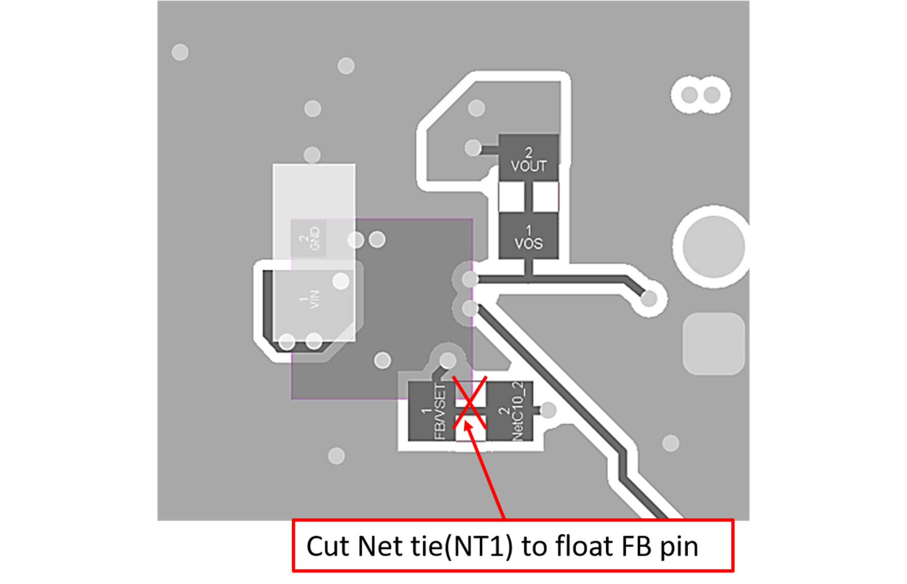
The TPS629203-Q1EVM is configured for external feedback as default with an output voltage of 3.3 V set by R1 and R2. Additionally, if the internal feedback (VSET) configuration is used, the user can cut net tie NT1 located on the back of the board. Figure 3-1 shows this modification. This will float the FB pin, resulting in a 3.3-V output voltage using the internal VSET. Resistors R1 and R2 can also be changed to set the output voltage between 0.6 V and 5.5 V. See the TPS629203-Q1 data sheet for recommended values. R2 was populated with 34 k such that if the internal (VSET) is chosen while R1 is removed, the device will regulate to 1.8-V output voltage.
WARNING: If the output voltage is increased, make sure the voltage rating of output capacitor C5 is sized appropriately.
GUID-ECE21167-6F51-4154-82D8-55DF45EE6DAD-low.pngFigure 3-1 Internal Feedback (VSET) Configuration Board Modification