SLVUCF2
March 2022
TPS55289
Trademarks
1
Introduction
1.1
Performance Specification
1.2
Modification
1.2.1
Modification
2
Connector, Test Point, and Jumper Descriptions
2.1
Connector and Test Point Descriptions
2.2
Jumper Configuration
2.2.1
JP1 (ENABLE)
2.2.2
JP6 (SYNC)
2.2.3
JP7 (I2C Target Address Selection)
2.2.4
JP8 (Internal or External VCC Selection)
2.2.5
JP9 and JP10 (External Feedback and Internal Feedback Selection)
3
Test Procedure
4
Software User Interface
4.1
Install USB2ANY Explorer
4.2
GUI Installation
4.3
Interface Hardware Setup
4.4
User Interface Operation
4.5
Register Map Screen
5
Schematic, Bill of Materials, and Board Layout
5.1
Schematic
5.2
List of Materials
5.3
Board Layout
5.3
Board Layout
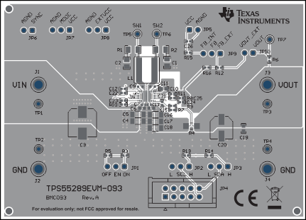
Figure 5-2
TPS55289EVM-093 Top-Side Layout
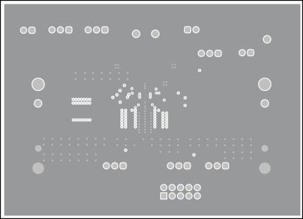
Figure 5-3
TPS55289EVM-093 Inner Layer1
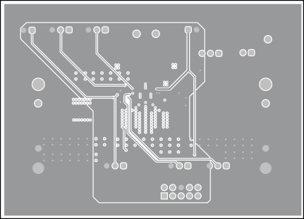
Figure 5-4
TPS55289EVM-093 Inner Layer2
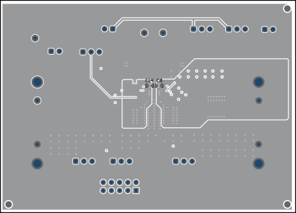
Figure 5-5
TPS55289EVM-093 Bottom-Side Layout