SLVUCF2 March 2022 TPS55289
4.4 User Interface Operation
The TPS55289EVM board can be enabled to work by the following steps:
- Set JP1 to the ON position. Turn on the power supply.
- Open the TPS55289EVM GUI.
- Click the auto connect button on the target address widget
(Figure 4-2). It will automatically check for target addresses
(0x74, 0x75) and connect the GUI with the device. After the
GUI and device are connected, the GUI reads all eight
registers and shows a notification (Figure 4-3).
 Figure 4-2 GUI
Auto Connect Button
 Figure 4-3 GUI
Auto Connect Notification
 - Click the start button. It will show the GUI user interface of
TPS55289EVM-093 (Figure 4-4).Figure 4-4 GUI User Interface of TPS55289EVM-093
- Click the Enable button (Figure 4-5). The default output voltage is 5 V.Figure 4-5 ENABLE Button
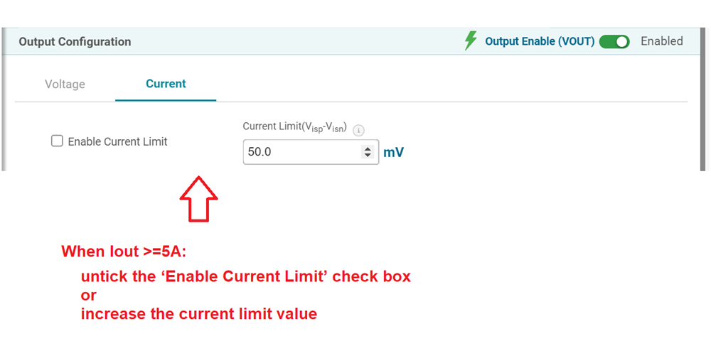
- Set the output voltage, current limit point, and so forth
according to the design target. If the maximum load current
is ≥ 5 A, uncheck the ‘Enable Current Limit’ check box or
increase the current limit value (Figure 4-6).
 Figure 4-6 Output Current Limit Point Setting