SLVUCK1 April 2024 TPS7H4011-SP
5.4 Load Step
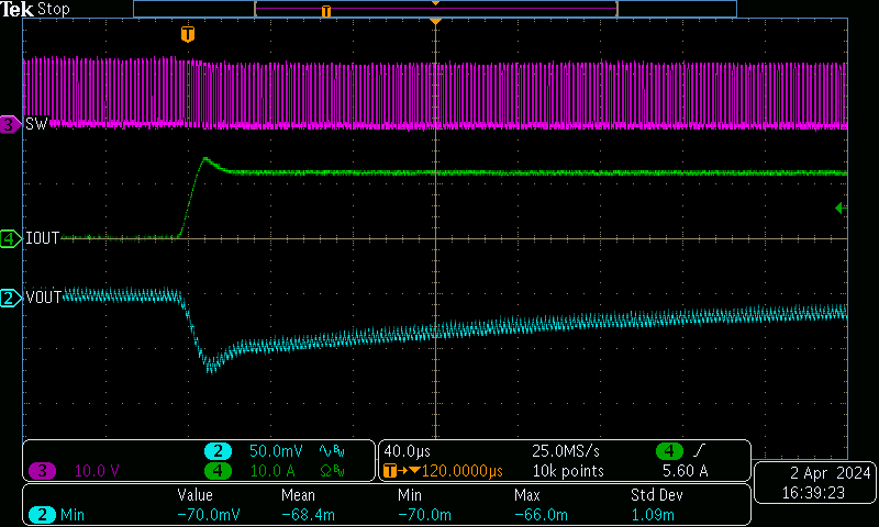
 Figure 5-3 Transiant Response to Load Step 100mA to 12A at 8A/µs
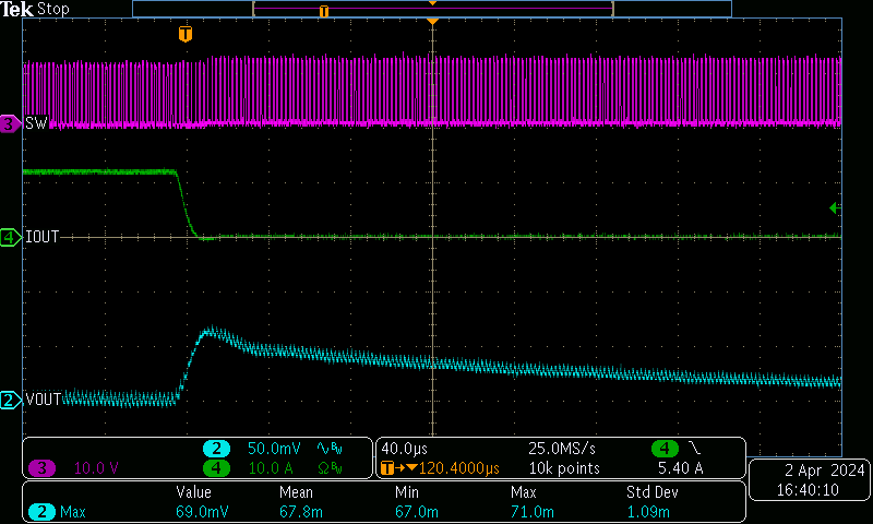
 Figure 5-4 Transiant Response to Load Step 12A to 100mA at 8A/µs
SLVUCK1 April 2024 TPS7H4011-SP
 Figure 5-3 Transiant Response to Load Step 100mA to 12A at 8A/µs
 Figure 5-4 Transiant Response to Load Step 12A to 100mA at 8A/µs