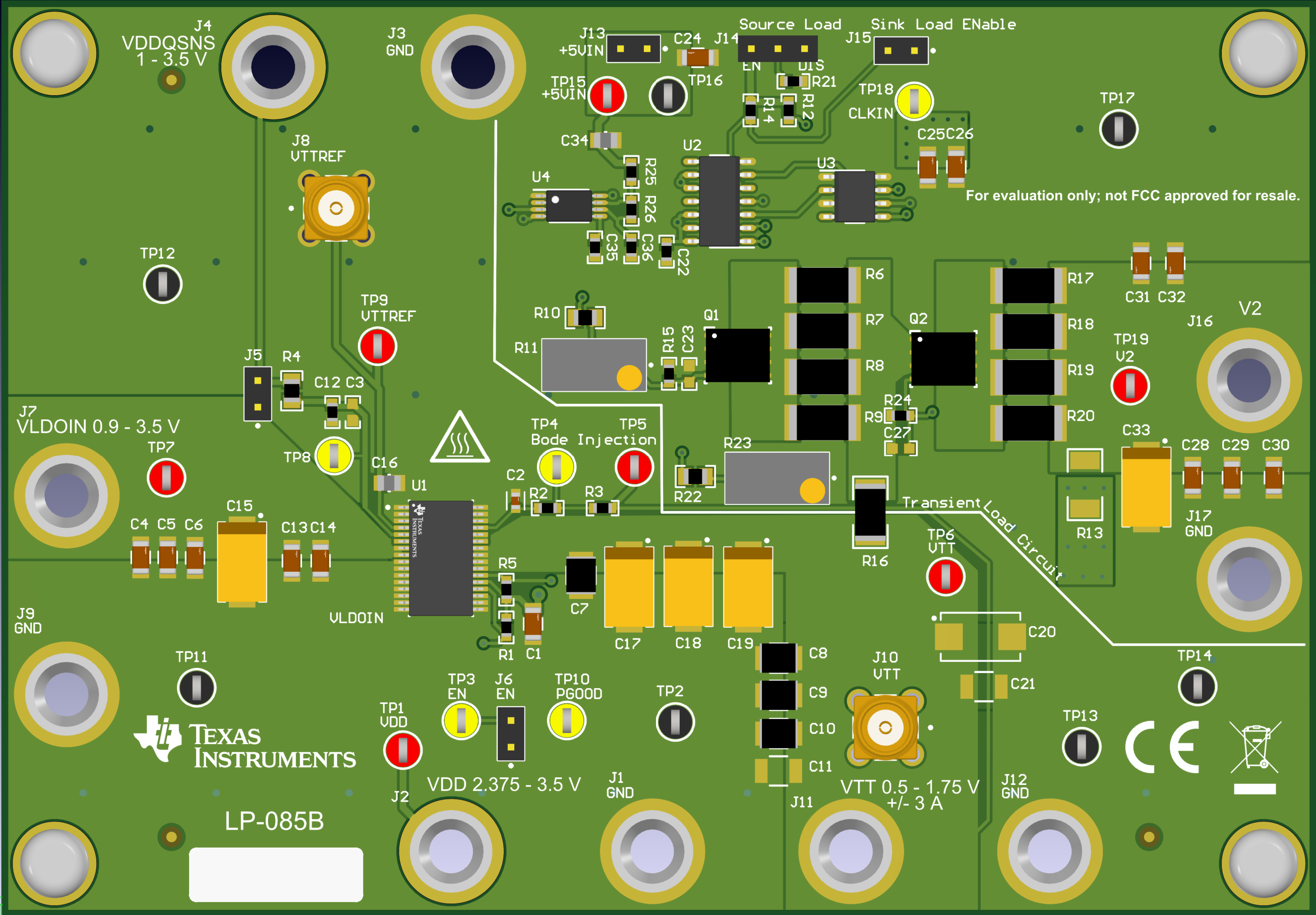
TPS7H3302EVM (LP085)
1 Abstract
This user’s guide describes operational use of the TPS7H3302EVM evaluation module (EVM) as a reference design for engineering demonstration and evaluation of the TPS7H3302-SEP, a 3-A sink and source DDR termination LDO regulator. This user's guide provides details about the EVM, the configuration, schematics, and bill of materials (BOM).
Trademarks
All trademarks are the property of their respective owners.
1 Introduction
The TPS7H3302EVM-SEP (LP085) evaluation board is designed to evaluate the performance and characteristics of TI's radiation tolerant DDR/DDR2/DDR3/DDR3L/DDR4 termination regulator, the TPS7H3302-SEP.
 Figure 1-1 TPS7H3302EVM Board (Top View)
2 Description
The TPS7H3302-SEP is a radiation-tolerant double data rate (DDR) ±3 A termination regulator with built-in VTTREF buffer. The regulator is specifically designed to provide a complete, compact, low-noise device for space DDR termination applications such as single board computers, solid state recorders, and payload processing.
The TPS7H3302-SEP supports DDR VTT termination applications using DDR, DDR2, DDR3, and DDR4. The fast transient response of the TPS7H3302-SEP VTT regulator allows for a very stable supply during read and write conditions. During transients, the fast tracking feature of the VTTREF supply minimizes any voltage offset between VTT and VTTREF. To enable simple power sequencing, both an enable input and a power-good output (PGOOD) have been integrated into the TPS7H3302-SEP. The open-drain output of the PGOOD terminal is compatible with being tied to other open-drain outputs, which facilitates the monitoring of a group supplies; such that a solitary GPIO pin can detect when all supplies are in regulation. The enable signal also discharges VTT during suspend to RAM (S3) power down mode.
2.1 Related Information
- TPS7H3302-SEP data sheet (SLVSGX6)
2.2 Typical Applications
The EVM is used in the following applications:
- Radiation-tolerant DDR power applications
- Memory termination regulator for DDR, DDR2, DDR3, and DDR4
2.3 Features
This EVM has the following features:
- Input core voltage VDD supports 2.5-V rail and 3.3-V rail
- VLDOIN, VDDQ voltage range: 0.9 V–3.5 V
- Dynamic performance evaluation features:
- Sink and source integrated load switches for transient load step emulation
- Configurable load step
and slew rate control by on-board resistorsCAUTION: The default EVM configuration using the built-in transient test circuit supports testing the DDR4 at ±1.5 A, DDR3 at ±1.875 A, DDR2 at ±2.25 A. To evaluate the DDR node, or different currents for DDR2, DDR3, DDR3L, and DDR4 the total resistance of resistors R6-R9, and R17-R20 needs to be changed to not exceed device maximum ratings.
- Jumper J14 (pins 1 and 2) for device enable. (enabled without J14 installed)
- Convenient test points for probing PGOOD, CLK_IN, and loop response testing
- Optional placeholders for VDDQSNS to VLDOIN filter when not using independent VDDQSNS source
2.4 Performance Specification Summary
Table 2-1 lists the EVM performance specifications. See data sheet (SLVSGX6) for complete specifications.
| Specification | Test Conditions | MIN | TYP | MAX | Unit |
|---|---|---|---|---|---|
| Input voltage range, (VVIN) | 2.375 | 3.3 | 3.5 | V | |
| VDDQSNS voltage range (VVDDQSNS) | 1 | 3.5 | |||
| VLDOIN voltage range (VVLDOIN) | 0.9 | 3.5 | |||
| VTT Termination Voltage | |||||
| DDR | VTT | 1.25 | |||
| VTTREF | 1.25 | ||||
| DDR2 | VTT | 0.9 | |||
| VTTREF | 0.9 | ||||
| DDR3 | VTT | 0.75 | |||
| VTTREF | 0.75 | ||||
| DDR4 | VTT | 0.6 | |||
| VTTREF | 0.6 | ||||
| Termination current (IVTT) | –3 | 3 | A | ||
| Reference current (IVTTREF) | –10 | 10 | mA | ||