SLVUCK2A january 2023 – april 2023 TPS7H3302-SEP
3.3.2 EVM Transient Test
A transient test setup circuit is incorporated as part of the EVM.
The built-in transient load switches (with both sinking and sourcing capability) are available to emulate the sink or source transient behavior to evaluate the dynamic performance. For ease of use, both load step and transient timing can be modified by on-board resistors. The EVM has two sets of four parallel 1.6 Ω resistors connected for transient load for both the VTT to GND, and VTT to V2 to accommodate both sourcing and sinking evaluation. Optionally, resistor R13 can be populated with zero Ω resistor to utilize VLDOIN as source for sinking transients. This method can cause a poor response due to transients introduced on VLDOIN, especially if VDDQSNS is tied to VLDOIN.
- Remove any external loads.
- Place jumper J14 (pins 2 and 3) source load selector (labeled "EN").
- Place jumper J15 (pins 1 and 2) sink load selector.
- Remove jumper J5 to isolate VDDQSNS from VLDOIN.
- Apply 2.5 V to VIN.
- Apply 1.5 V to J7/J9 VLDOIN.
- Apply 1.5 V to J16/J17 V2 (this is the source for the sinking transients).
- Apply 1.5 V to J4/J3 VDDQSNS. If testing with VDDQSNS is not isolated from VLDOIN, install J10, and only apply to VLDOIN (with reduced performance).
- Monitor VTT to verify VTT voltage is present. VTT is approximately 750 mV.
- Apply 5 V to J13 (pin 2 [+], pin 1 [–]) (or by TP15, TP16), providing power to the transient load setup.
- Monitor VTT at J10 using a scope to see transient results.
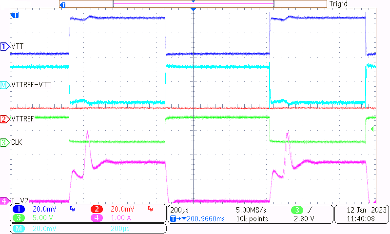
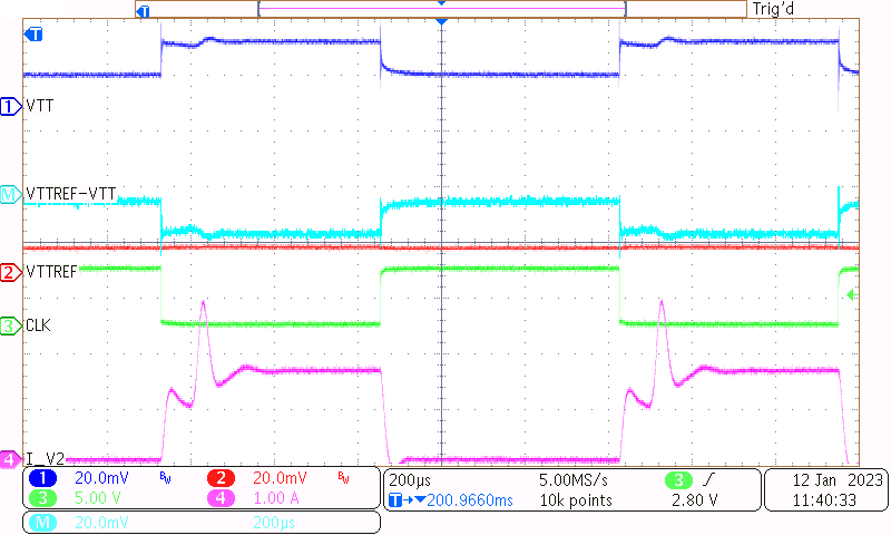
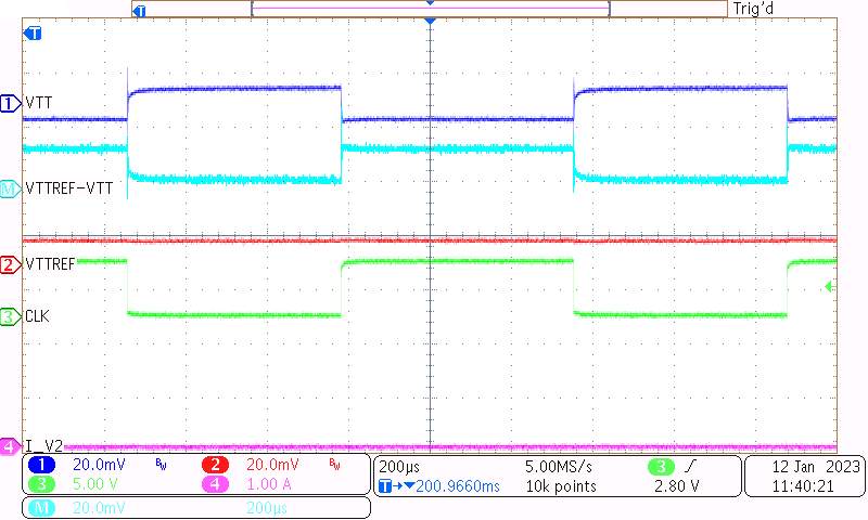
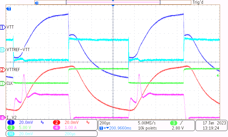
The following plots show the results of using the transient circuit configured for DDR3 voltages. All the plots have VTT and VTTREF shown with 750 mV offset applied. In addition to VTT and VTTREF, the plots include the clock signal (CLK), the math function of the difference of VTTREF - VTT, and the current measurements of V2. Note, that V2 only represents the current when the device is sinking. Thus, during the sourcing, this current is zero. During sourcing, a near identical current is present through VLDOIN.
Figure 3-5 shows the response of the circuit with both sinking and sourcing enabled.
Figure 3-5 shows the response of the circuit with only sinking transients applied. This method can be tested by only having shunt on J15 and no shunt on J14.
Figure 3-6 shows the response of the circuit with only sourcing transients applied. This method can be tested by only having shunt on EN pins of J14, and no shunt on J15.
Figure 3-7 shows the transient response with VDDQSNS not isolated from VLDOIN with both sinking and sourcing enabled. Transients on VLDOIN also influences VDDQSNS and cause undesirable disturbances. Transient response can be improved with implementation of a filter on VDDQSNS from VLDOIN. The filter can be implemented by replacing components for R4, and C3. Note the large fluctuation on VTTREF due to VLDOIN and hence VDDQSNS transients.
 Figure 3-4 DDR3 Scope Plot Response With Both
Sinking and Sourcing Enabled and VDDQSNS Isolated.
 Figure 3-5 DDR3 Scope Plot of Response with 1.875
A Sinking Only with Isolated VDDQSNS
 Figure 3-6 DDR3 Scope Plot of Response with 1.875
A Sourcing Only with Isolated VDDQSNS
 Figure 3-7 DDR3 Scope Plot of Response With 1.875
A Sinking and Sourcing With Non-Isolated VDDQSNS