SLVUCN2A October 2023 – August 2024 DRV3901-Q1
6.2 Addressable SPI
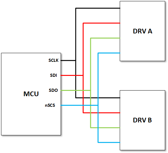
Addressable SPI allows SPI communication with both drivers simultaneously. In this mode, one nSCS signal is connected to both drivers. Diagram in Figure 6-2 shows the SPI connections for addressable SPI. The register map will display the register values of the selected driver. To write to a specific driver, it has to be selected in the GUI.
 Figure 6-2 Addressable SPI
Diagram
Figure 6-2 Addressable SPI
DiagramIn order for communication to be successful with both drivers, the following has to be done:
- The nFAULT/NAD resistor of each driver has to be different. The NAD resistors for each driver are selected in headers J3 and J8 (Table 2-2). The resistor value needs to match the resistor selected in the GUI .
Note: The NAD/nFAULT resistors are latched during
DRV3901-Q1 power up. Ensure that the desired resistors for each driver are selected
in the EVM before powering up the board.