SLVUCO4 October 2023 TPS62916
1.2.6 Loop Response Measurement
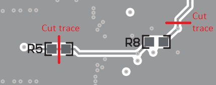
The loop response can be measured with simple changes to the circuitry. First, cut the short section of trace on the bottom layer between the pads of R5 resistor. Second, cut the trace on the bottom layer that connects to R8. Figure 1-1 shows these changes. Third, install a 49.9-Ω resistor across R5 pads on the back of the PCB and install a 0-Ω resistor across R8 pads on the back of the PCB. The pads are spaced to allow installation of a 0603-sized resistors. Lastly, replace the ferrite bead (FB1) with a 0-Ω resistor and remove any second LC stage output capacitors C19 to C23. The second LC filter must be removed to break the complete feedback loop and measure the loop response. With these changes, an AC signal (10-mV, peak-to-peak amplitude recommended) can be injected into the control loop across the added 49.9-Ω resistor. Figure 3-2 shows the results of this test.
 Figure 1-1 Loop Response Measurement Modification (Bottom Layer)