SLVUCP4 November 2023
2.3 Jumper Information
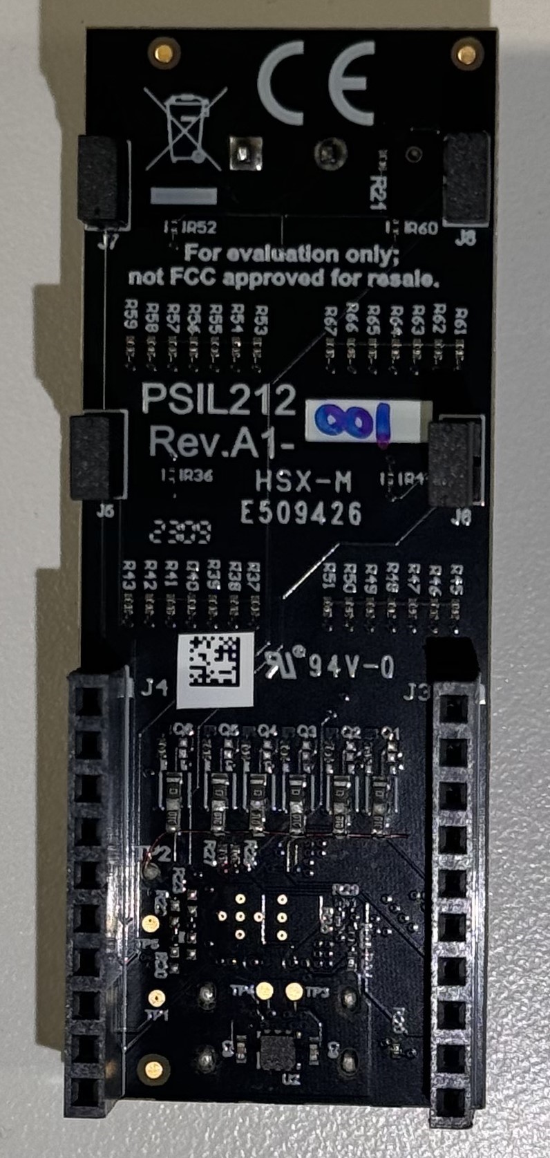
Four jumpers are present on the TPS25730EVM, as shown below, with each jumper connecting a set of switches to the corresponding ADCIN pin on the TPS25730. Jumper J5 connects the switch-set labeled ADCIN4 to the ADCIN4 pin of the TPS25730. Similarly, J6 is connected to ADCIN3, J7 is connected to ADCIN2, and J8 is connected to ADCIN1.
 Figure 2-1 TPS25730EVM Bottom View of the
Jumper Locations
Figure 2-1 TPS25730EVM Bottom View of the
Jumper LocationsJ5 can be removed and resistors populated on the board for a permanent ADCIN4 configuration. R33 is the resistor connected to ground in the ADCIN4 resistor divider and R25 is the resistor connected to LDO_3V3 in the ADCIN4 resistor divider. Populating these resistors with values that correspond to the same ADCIN decoded value as configured with the ADCIN4 switch set provides the same configuration for ADCIN4.
An analogous process can be followed for all four jumpers to permanently configure any ADCIN configuration. Table 3-1 details which resistor pads correspond to which ADCIN switch set and jumper.
| Jumper | ADCIN Input | Pull-up resistor | Pull-down resistor |
|---|---|---|---|
| J8 | ADCIN1 | R22 | R30 |
| J7 | ADCIN2 | R23 | R31 |
| J6 | ADCIN3 | R24 | R32 |
| J5 | ADCIN4 | R25 | R33 |
| DIV = RDOWN / (RUP + RDOWN) | Without Using RUP or RDOWN | ADCINx Decoded Value | ||
|---|---|---|---|---|
| MIN | Target | MAX | ||
| 0 | 0.0114 | 0.0228 | tie to GND | 0 |
| 0.0229 | 0.0475 | 0.0722 | N/A | 1 |
| 0.0723 | 0.1074 | 0.1425 | N/A | 2 |
| 0.1425 | 0.1899 | 0.2372 | N/A | 3 |
| 0.2373 | 0.3022 | 0.3671 | N/A | 4 |
| 0.3672 | 0.5368 | 0.7064 | tie to LDO_1V5 | 5 |
| 0.7065 | 0.8062 | 0.9060 | N/A | 6 |
| 0.9061 | 0.9530 | 1.0 | tie to LDO_3V3 | 7 |