SLVUCS2A August 2024 – September 2024 TPS25763-Q1
4.1 Known Hardware or Software Limitations
USB 2.0 MUX Disabled
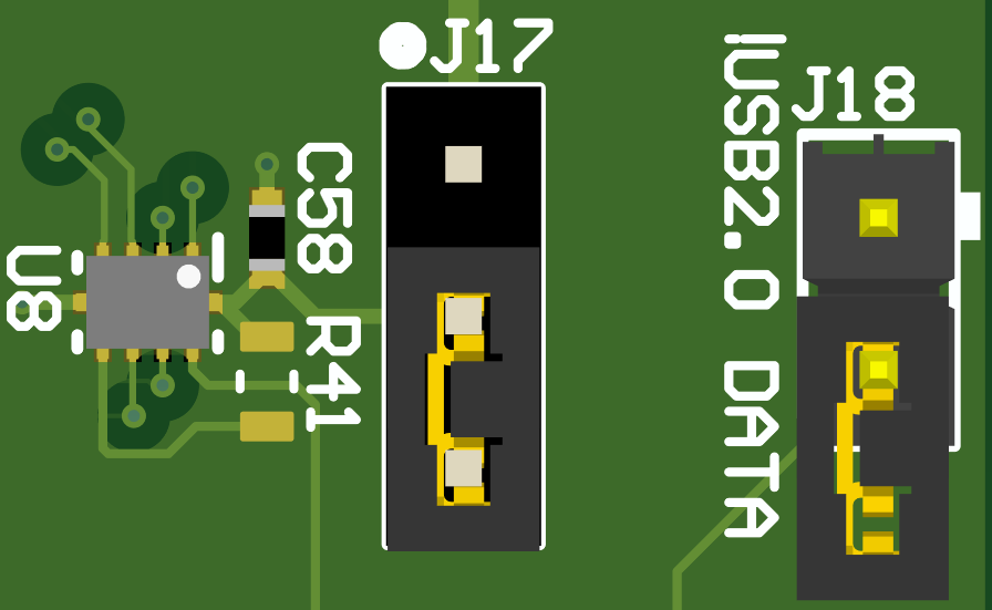
TS3USB221A-Q1 USB 2.0 data MUX /OE pin is misconfigured. This prevents legacy charge handshakes and firmware updates over the Type-C port from working as intended. To fix this, short the bottom pad of R41 (/OE) to the top pad of C58 (GND).
 Figure 4-1 TS3USB221A-Q1 /OE Input Correction
Dual Role Power (DRP) Circuit
When configured as a DRP system, a 100Ω resistor must be placed in parallel with the NFET load switch between CSN/OUT and the Type-C receptacle. The required resistance is 100Ω with ±5% tolerance and 0.25W rating. This resistor can be installed by the user as R8 on the EVM.
 Figure 4-2 DRP Simplified Bypass Resistor Circuit
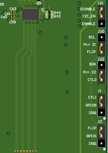
J2 IRQ2 Silk Screen Error
The silk screen label for pin 1 of J2 is mislabeled and reads IRQ2.
 Figure 4-3 J2 IRQ2 Silk Screen Error
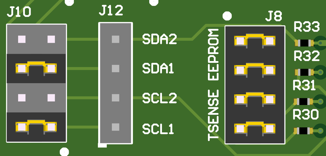
J8 Silk Screen Error
The silk screen label for EEPROM and TSENSE are reversed. Onboard EEPROM I2C1 pullups are rows 3 and 4 (pins 5-6 and 7-8), TMP75B-Q1 I2C1 pullups are rows 1 and 2 (pins 1-2 and 3-4).
 Figure 4-4 J8 Silk Screen Error