SLVUCT9 January   2024


  1.   1
  2.   Description
  3.   Features
  4.   Trademarks
  5. 1Evaluation Module Overview
    1. 1.1 Introduction
    2. 1.2 Kit Contents
    3. 1.3 Specification
      1. 1.3.1 Alternate Board Configurations
    4. 1.4 Device Information
  6. 2Hardware
    1. 2.1 Power Requirements
    2. 2.2 Important Usage Notes
    3. 2.3 Connector Descriptions
  7. 3Implementation Results
    1. 3.1 Default Configuration Results
    2. 3.2 Sequence UP and DOWN Thresholds
    3. 3.3 Delay Timer
    4. 3.4 Regulation Timer
    5. 3.5 Disabled Channels
    6. 3.6 Externally Induced System RESET
  8. 4Hardware Design Files
    1. 4.1 Schematics
    2. 4.2 PCB Layouts
    3. 4.3 Bill of Materials (BOM)
  9. 5Compliance Information
    1. 5.1 Compliance and Certifications
  10. 6Additional Information
    1. 6.1 Known Hardware Issues
  11. 7Related Documentation
  12. 8Revision History

Externally Induced System RESET

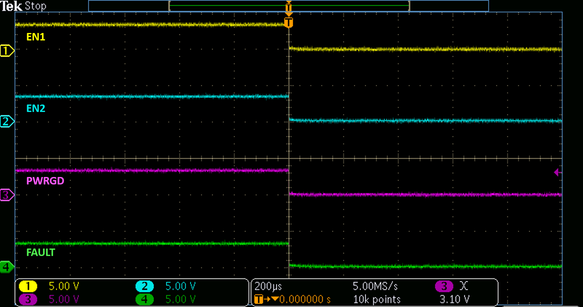
The following test was performed using a FET to ground the SENSE1 pin to induce a FAULT. This can be done if an external system RESET signal is desired by the user. CH3 and CH4 were disabled during this test for convenience of displaying the results. Applying 3.3V to the gate of the FET circuitry shown in the "Optional External Reset" section of the EVM Schematic induces the external RESET. If used, it is recommended to choose a FET with low leakage to minimize the error it introduces to the SENSEx ON and OFF thresholds.
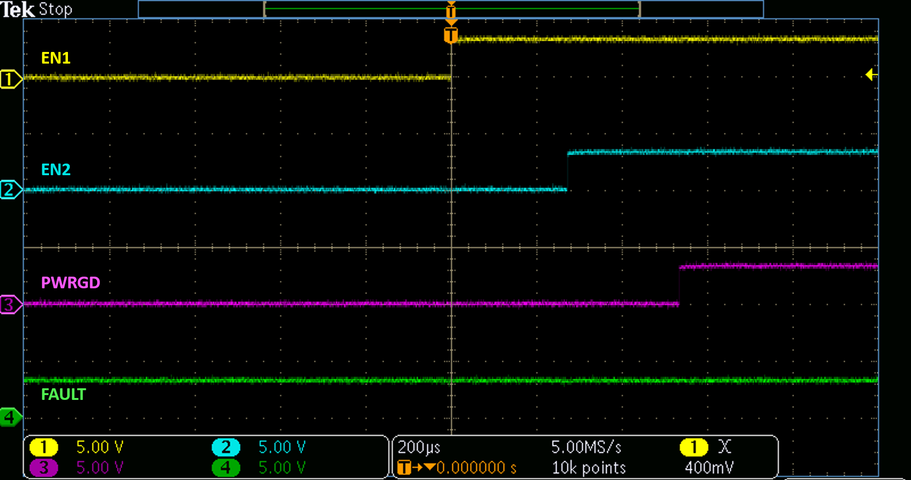
GUID-E0C64E43-7D34-42C5-AA18-D4414CF05814-low.pngFigure 3-15 Sequence UP
GUID-0B1D14B9-7939-4B54-B405-846BBF283E1A-low.pngFigure 3-16 External System RESET