SLVUCW0 June 2024 TPSM86837
4.2 PCB Layouts
This section provides a description of the TPSM86837EVM, board layout, and layer illustrations.
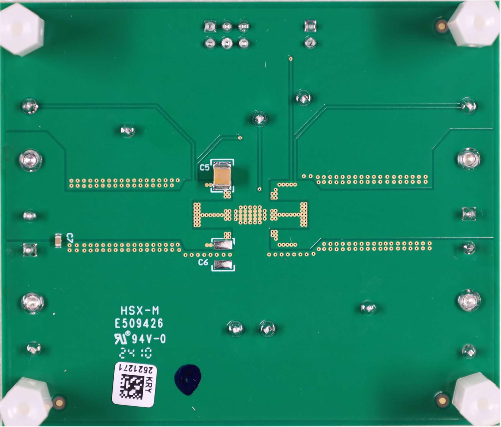
The board images are shown in Figure 4-2 and Figure 4-3. The board layouts are shown in Figure 4-4 to Figure 4-8. The top layer contains the main power traces for VIN, VOUT, and ground. Also on the top layer are connections for the pins of the TPSM86837, a large area filled with power ground (PGND), and a small area filled with analog ground (AGND). Most of the signal traces are also located on the top side. The input capacitors and output capacitors are located close to the device . The input and output connectors, test points, and most of the components are located on the top side. Middle layer 1, Middle layer 2, and the bottom layer are predominantly PGND planes. The additional two output capacitors are located on the bottom side.Figure 4-4 shows the AGND and PGND are connected at a single point on the top layer. The bottom layer contains the output voltage feedback trace, the connection to the VIN pin of the EN control, the connection to the Vout of PGood pin, and the connections of test points.
 Figure 4-2 TPSM86837EVM Front Photo
 Figure 4-4 Top Assembly
 Figure 4-6 Middle Layer 1
 Figure 4-8 Bottom Layer
 Figure 4-3 TPSM86837EVM Back Photo
 Figure 4-5 Top Layer
 Figure 4-7 Middle Layer 2