SLWS230E September 2011 – December 2015 TRF3765
PRODUCTION DATA.
- 1 Features
- 2 Applications
- 3 Description
- 4 Revision History
- 5 Pin Configuration and Functions
- 6 Specifications
- 7 Detailed Description
- 8 Application and Implementation
- 9 Power Supply Recommendations
- 10Layout
- 11Device and Documentation Support
- 12Mechanical, Packaging, and Orderable Information
8 Application and Implementation
NOTE
Information in the following applications sections is not part of the TI component specification, and TI does not warrant its accuracy or completeness. TI’s customers are responsible for determining suitability of components for their purposes. Customers should validate and test their design implementation to confirm system functionality.
8.1 Application Information
The TRF3765 is a wideband integer-N/Fractional-N frequency synthesizer with an integrated, wideband voltage-controlled oscillator (VCO). Programmable output dividers enable continuous frequency coverage from 300 MHz to 4.8GHz. Four separate differential, open-collector RF outputs allow multiple devices to be driven in parallel without the need of external splitters. TRF3765 is applicable to the wireless infrastructure standards such as CDMA, TDMA, WCDMA, LTE and Advanced-LTE. It can also be used in wireless point-to-point access and wireless local loop communication links.
8.2 Typical Application
Figure 77 shows an example block diagram for multi-band and multi-mode for 2G, 3G, and 4G cellular transmitters. By adopting DAC38J84 and TRF3720, number of transmitter can be increased up to 8 antenna system as each of DAC38J84 can supports 2 transmitters of I/Q pair and each of TRF3765 can provide 4 high sampling clocks with 4 DAC38J84 devices. TRF3720 is an IQ modulator with fully integrated PLL/VCO and LO frequency ranges from 300 MHz to 4.8 GHz.
This is a good example of improved transmitter diversity to service multiple users simultaneously. The internal PLL of TRF3765 can be used to generate four high sampling clocks up to 4.8 GHz.
 Figure 77. TRF3765 Application Block Diagram
8.2.1 Design Requirements
For this design example, use the input parameters in Table 18.
Table 18. Design Parameters
| DESIGN PARAMETER | EXAMPLE VALUE |
|---|---|
| Input voltage | 3.3 V |
| Current | 121 mA |
| Input reference frequency | 122.88 MHz |
| Output frequency | 900 MHz |
Table 19. Termination Requirements and Interfacing
| PIN | NAME | DESCRIPTION |
|---|---|---|
| 3 | DATA | 4WI data input: digital input, high impedance |
| 4 | CLOCK | 4WI clock input: digital input, high impedance |
| 5 | STROBE | 4WI latch enable: digital input, high impedance |
| 6 | READBACK | Readback output; digital output pins can source or sink up to 8 mA of current |
| 9 through 16 | LO_OUT | Local oscillator output: open-collector output. A pullup resistor is required, normally ac-coupled. Any unused output differential pairs may be left open. |
| 18 | EXTVCO_IN | External local oscillator input: high impedance, normally ac-coupled |
| 19 | EXTVCO_CTRL | Power-down control pin for optional external VCO; digital output pins can source or sink up to 8 mA of current |
| 30 | REF_IN | Reference clock input: high impedance, normally ac-coupled |
| 32 | LD | Lock detector digital output, as configured by MUX_CTRL; digital output pins can source or sink up to 8 mA of current |
8.2.2 Detailed Design Procedures
8.2.2.1 Power Supply
A clean power supply is critical to optimal phase noise performance of synthesizer. Linear power supplies are the best sources available. Switching power supplies degrade in-band phase noise by 10 dB compared to linear laboratory supplies. VCC3 can be used to drive VCC_TK, a 3.3-V or 5-V tolerant supply on the TRF3765. VCC_TK is normally driven by the 3.3 V VCC2 supply, but some applications perform better with 5 V supply on VCC_TK. A power supply filter can be used for TRF3765 and this filter reduces in-band frequency noise from a switching power supply so that external supply can drive 5 V on VCC_TK.
8.2.2.2 Loop Filter
Loop-filter components are also critical to optimal phase noise performance. The loop filter must be matched to the selected phase noise frequency detector (PFD) frequency. To use different PFD frequency, the loop-filter components must be updated. Below is an example of loop filter design.
8.2.2.3 Reference Clock
External oscillator or the output of PLL device can be installed for the reference clock input to TRF3765 device. The external reference clock is AC-coupled to the TRF3765 input pin. The range is reference frequency is from 0.5 MHz to 350 MHz. The minimum of reference input sensitivity is 0.2 Vpp and 3.3 Vpp for the maximum value.
8.2.3 Application Curves
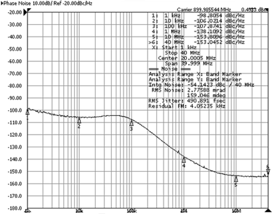
The phase noise performance of 900-MHz output is shown in Figure 78. Figure 79 shows phase noise performances from different power supplies such as 3.3 V, 2.7 V, 2.5 V, 2.2 V, 2.1 V and 2 V at room temperature.

