SLWU087E november 2013 – june 2023
- 1
- High Speed Data Converter Pro GUI
- Trademarks
- 1 Introduction
- 2 Software Start up
-
3 User Interface
- 3.1
Toolbar
- 3.1.1 File Options
- 3.1.2 Instrument Options
- 3.1.3 Data Capture Option
- 3.1.4
Test Options
- 3.1.4.1 Notch Frequency Bins
- 3.1.4.2 2 Channel Display and Cursor Lock
- 3.1.4.3 Analysis Window Markers
- 3.1.4.4 X-Scale in Time
- 3.1.4.5 Y-Scale in Voltage
- 3.1.4.6 Other Frequency Options
- 3.1.4.7 NSD Marker
- 3.1.4.8 Phase Plot
- 3.1.4.9 Phase in Degree
- 3.1.4.10 Histogram
- 3.1.4.11 Disable User Popups
- 3.1.4.12 HSDC Pro Lite Version
- 3.1.5 Help
- 3.2 Status Windows
- 3.3 Mode Selection
- 3.4 Device Selection
- 3.5 Skip Configuration
- 3.6 Capture Button (ADC Mode Only)
- 3.7 Test Selection (ADC Mode only)
- 3.8 DAC Display Panel (DAC Mode only)
- 3.9 I/Q Multi-Tone Generator
- 3.1
Toolbar
- 4 ADC Data Capture Software Operation
- 5 TSW1400 Pattern Generator Operation
- 6 TSW14J58 Functional Description
- 7 TSW14J57 Functional Description
- 8 TSW14J56 Functional Description
- 9 TSW14J50 Functional Description
- 10TSW14J10 Functional Description
- A Signal Processing in High Speed Data Converter Pro
- B History Notes
- C Revision History
3.1.4.1 Notch Frequency Bins
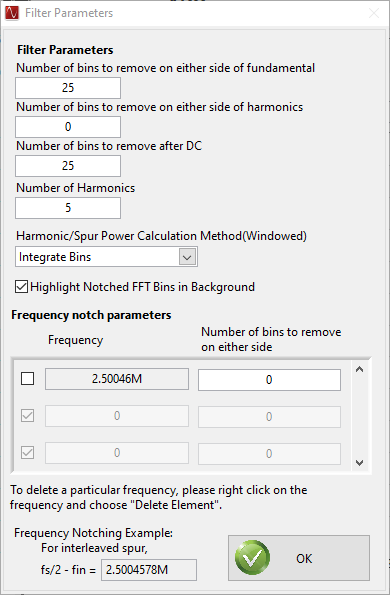
The Notch Frequency Bins option allows the user to remove a number of bins from the SNR calculation of the input frequency around the fundamental, DC and a predetermined number of harmonics. The default values for these settings when capturing data using Blackman window mode is 25, 0, 25, and 5, as shown in Figure 3-18. When the capture mode is set to Rectangular mode, the default values are 0, 0, 1, 5.
 Figure 3-18 Notch Frequency Bin Removal
By default, the noise calculations for SNR and SINAD are based on the FFT of the captured data with the Notch Filter parameters applied. The first FFT bin at DC is not used because the first bin contains DC offset and thus does not effect AC parameters or AC performance. The rest of the FFT bins out to the Nyquist frequency are included in the calculation of the total noise.
The Harmonic/Spur Power Calculation Method(Windowed) button allows the user to either Integrate the Bins or Don't Integrate the bins. When "Integrate Bins" is selected, the neighboring bins are also included in the harmonic and spur calculations. Apart from the harmonic frequency bin, its neighboring bins will also be used for harmonic power calculation.
When "Don't Integrate" is selected, the neighboring bins are not included in the harmonic and spur calculations. Only the single harmonic frequency bin will be used for the harmonic power calculation.
This option will also affect the FFT filtering. In "Integrate" mode, neighboring bins of the harmonics will not be notched.
There is also an option to notch out bins around a user defined frequency. The default sets the number of bins to 0. If the clock input is mixing with the input signal, there may be a spur at fs/2 - fin, where fs is the ADC sample frequency and fin is the input frequency. This option could be used to notch this spur from the results if desired. Select the top entry to enable notching for this frequency. Select the other boxes below this one to notch out bins around user defined frequencies. If the user enters a "1" for number of bins to be removed, 1 bin will be removed at the frequency entered and one bin will be removed from each side of this frequency. If the user enters a "2", the bin at the frequency will be removed along with 2 bins on each side of the frequency, and so on. The GUI calculates the fs/2-fin frequency for informational use only in the equation box. The default value is "0" since the default value of both fs/2 and fin is "0". This value is updated when the user enters the ADC sample rate and ADC Input target frequency in the main GUI panel.
The “Highlight Notched FFT Bins in Background” option is used to highlight the area of notched frequency bins in the FFT display window.