SLWU087E november 2013 – june 2023
- 1
- High Speed Data Converter Pro GUI
- Trademarks
- 1 Introduction
- 2 Software Start up
-
3 User Interface
- 3.1
Toolbar
- 3.1.1 File Options
- 3.1.2 Instrument Options
- 3.1.3 Data Capture Option
- 3.1.4
Test Options
- 3.1.4.1 Notch Frequency Bins
- 3.1.4.2 2 Channel Display and Cursor Lock
- 3.1.4.3 Analysis Window Markers
- 3.1.4.4 X-Scale in Time
- 3.1.4.5 Y-Scale in Voltage
- 3.1.4.6 Other Frequency Options
- 3.1.4.7 NSD Marker
- 3.1.4.8 Phase Plot
- 3.1.4.9 Phase in Degree
- 3.1.4.10 Histogram
- 3.1.4.11 Disable User Popups
- 3.1.4.12 HSDC Pro Lite Version
- 3.1.5 Help
- 3.2 Status Windows
- 3.3 Mode Selection
- 3.4 Device Selection
- 3.5 Skip Configuration
- 3.6 Capture Button (ADC Mode Only)
- 3.7 Test Selection (ADC Mode only)
- 3.8 DAC Display Panel (DAC Mode only)
- 3.9 I/Q Multi-Tone Generator
- 3.1
Toolbar
- 4 ADC Data Capture Software Operation
- 5 TSW1400 Pattern Generator Operation
- 6 TSW14J58 Functional Description
- 7 TSW14J57 Functional Description
- 8 TSW14J56 Functional Description
- 9 TSW14J50 Functional Description
- 10TSW14J10 Functional Description
- A Signal Processing in High Speed Data Converter Pro
- B History Notes
- C Revision History
3.1.3.2 Trigger Option
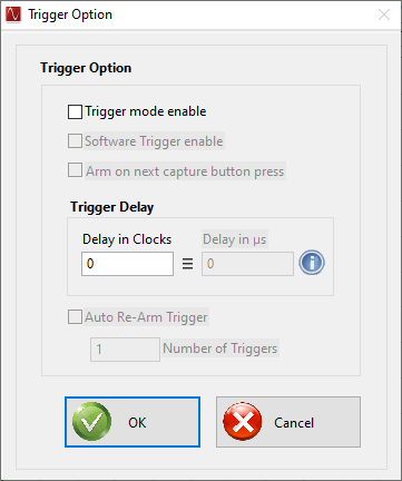
Clicking on the Trigger Option will open a new panel as shown in Figure 3-10. This option is not available for the TSW1405/06. The GUI provides four options of capturing data using a trigger function. Selecting Trigger mode enable will arm the TSW14xxx to accept an external trigger.
 Figure 3-10 Trigger Option
With both enables selected, the capture button on the main panel of the GUI now changes from "Capture" to “Generate Trigger”. When the user clicks on this button, the GUI sends a CMOS logic level (1.8 VDC) active high pulse to the four SMA connectors labeled SYNC1, SYNC2, SYNC3, and SYNC4 on the TSW1400. On the TSW14J5x, these are labeled as TRIG_OUT_A, TRIG_OUT_B, and TRIG_OUT_C. This signal can be used to trigger other TSW14xxx EVMs or the same TSW14xxx. To use this rising edge to trigger the same TSW14xxx, the user must connect a cable from the SMA labeled as “EXT_TRG_INPUT” SMA (J11) on the TSW1400 ("TRIG_IN", SMA J13 on the TSW14J5x) to one of the SYNC (TRG_OUT) SMA's. Without this connection, the GUI never detects a trigger and reports “No trigger occurred” a short time after the user has clicked on the "Generate Trigger" button. Once a trigger is detected, the GUI will do a capture.
Another trigger option is to use an external trigger source. To use this mode, only select “Trigger mode enable”. When this mode is selected, the status button located at the bottom of the main GUI screen will display “TRIGGER ARMED” in yellow and the capture button will display “Read DDR Memory”. The software is now waiting for a CMOS logic low to high transition to occur on the “EXT_TRG_INPUT” (TRG_IN) input SMA. Once this occurs, a data capture will occur. The user will now click on the “Read DDR Memory” button to display the captured data. If the user clicks on this button before a trigger occurred, a short time later a “No trigger occurred” message appears. If the external trigger is a continuous event, the GUI will not do a new capture until the user clicks on "Read DDR Memory". This causes the software to display the results from the first trigger event and reload the memory with new data on the next rising edge of the external trigger input.
Another trigger option involves selecting both "Trigger mode enable" and "Arm on next capture button press". With these two selected, the software will do a capture on the next rising edge detected on EXT_TRG_INPUT/TRIG_IN connectors only after the user clicks on the "capture" button. This mode comes in handy if there are multiple trigger pulses arriving but the user does not want to trigger until a certain time later. If a trigger is not detected within about 12 seconds after clicking on capture, the software will time out and report no trigger detected.
When using the trigger capture mode, the user has an option to capture data a fixed amount of samples after the capture has actually started. This is useful for devices that have a “High Resolution Burst mode”, where it takes several clock cycles to occur before valid samples are available. This delay is determined by the value entered in the “Trigger CLK Delays” box. The default value is “0”. The user can enter a value from 0–7 with the corresponding sample delay shown in Table 3-1. Note that the delay is also based on the number of channels captured. For example, if a user selects a Trigger Delay of “2” and is capturing data from 2 Channels, after a trigger is detected by the GUI, the data capture starts. With this delay setting though, the first data sample used by the GUI will be the 81th sample from the ADC after the trigger occurred.
Another trigger option involves selecting both “Trigger mode enable” and “Auto Re-Arm Trigger”. With these two selected, the TSW14xxx EVM captures the configured amount of samples (“# of samples per channel”, from the Capture Option). For every trigger pulse, (CMOS logic low to high transition that occurs on the “EXT_TRG_INPUT” (TRIG_IN, TSW14J5x) SMA.) and accumulate the captured samples in the DDR memory until the defined numbers of “Number of Triggers” is completed.
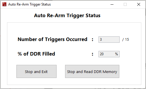
When using this capture mode, the status button located at the bottom of the main GUI screen displays “TRIGGER ARMED” in yellow and the capture button displays “Show Trigger Status”. Clicking on the “Show Trigger Status” button opens up a popup window displaying the status of the trigger operations with “Number of Triggers Occurred” and “% of DDR Filled”. Clicking on the “Stop and Exit” button stops the current capture operations without reading the captured sample. Clicking on the “Stop and Read the DDR Memory” button stops the current capture operations and read the captured samples from the DDR. After the configured Number of Triggers occurs and required amount of DDR gets filled, the “Stop and Read the DDR Memory” button displays “Read DDR Memory” and clicking on the same reads the captured samples from the DDR.
 Figure 3-11 Auto Re-Arm Trigger Status Window
For DAC mode, with both enables selected, the send button on the main panel of the GUI now changes from "Send" to “Generate Trigger”. When this button is clicked, the GUI sends a CMOS logic high level (3 VDC) to the four SYNC SMAs on the TSW1400 and the three TRIG_OUT SMAs on the TSW14J5x. This signal can trigger other TSW14xxx EVMs or the same TSW14xxx. A cable must be connected from the “EXT_TRG_INPUT” (TRIG_IN, TSW14J5x) SMA to one of the SYNC (TRIG_OUT, TSW14J5x) SMAs to use this rising edge to trigger the same TSW14xxx. Without this connection, the GUI never sends the data from the memory.
| Trigger Delay | Number of Samples Skipped Per Channel | |||
|---|---|---|---|---|
| 1 Channel | 2 Channel | 4 Channel | 8 Channel | |
| 1 | 80 | 40 | 20 | 10 |
| 2 | 160 | 80 | 40 | 20 |
| 3 | 240 | 120 | 60 | 30 |
| 4 | 320 | 160 | 80 | 40 |
| 5 | 400 | 200 | 100 | 50 |
| 6 | 480 | 240 | 120 | 60 |
| 7 | 560 | 280 | 140 | 70 |
Another trigger option involves selecting both “Trigger mode enable” and “Auto Re-Arm Trigger”. With these two selected the TSW14xxx EVM captures the configured amount of samples (“# of samples per channel”, from the Capture Option) for every trigger pulse (CMOS logic low to high transition that occurs on the “EXT_TRG_INPUT” (TRIG_IN, TSW14J5x) SMA.) and accumulate the captured samples in the DDR memory until the defined numbers of “Number of Triggers” is completed.
When using this capture mode, the status button located at the bottom of the main GUI screen displays “TRIGGER ARMED” in yellow and the capture button displays “Show Trigger Status”. Clicking on the “Show Trigger Status” button opens up a popup window displaying the status of the trigger operations with “Number of Triggers Occurred” and “% of DDR Filled”. Clicking on the “Stop and Exit” button stops the current capture operations without reading the captured sample. Clicking on the “Stop and Read the DDR Memory” button stops the current capture operations and read the captured samples from the DDR. After the configured Number of Triggers occurs and required amount of DDR gets filled, the “Stop and Read the DDR Memory” button displays “Read DDR Memory” and clicking on the same reads the captured samples from the DDR.
For DAC Auto Re-Arm Trigger mode, when the board receives a trigger signal at “EXT_TRG_INPUT” (TRIG_IN, TSW14J5x) SMA, the samples from the start index is sent out to the DAC from the FPGA.