SLWU087E november 2013 – june 2023
- 1
- High Speed Data Converter Pro GUI
- Trademarks
- 1 Introduction
- 2 Software Start up
-
3 User Interface
- 3.1
Toolbar
- 3.1.1 File Options
- 3.1.2 Instrument Options
- 3.1.3 Data Capture Option
- 3.1.4
Test Options
- 3.1.4.1 Notch Frequency Bins
- 3.1.4.2 2 Channel Display and Cursor Lock
- 3.1.4.3 Analysis Window Markers
- 3.1.4.4 X-Scale in Time
- 3.1.4.5 Y-Scale in Voltage
- 3.1.4.6 Other Frequency Options
- 3.1.4.7 NSD Marker
- 3.1.4.8 Phase Plot
- 3.1.4.9 Phase in Degree
- 3.1.4.10 Histogram
- 3.1.4.11 Disable User Popups
- 3.1.4.12 HSDC Pro Lite Version
- 3.1.5 Help
- 3.2 Status Windows
- 3.3 Mode Selection
- 3.4 Device Selection
- 3.5 Skip Configuration
- 3.6 Capture Button (ADC Mode Only)
- 3.7 Test Selection (ADC Mode only)
- 3.8 DAC Display Panel (DAC Mode only)
- 3.9 I/Q Multi-Tone Generator
- 3.1
Toolbar
- 4 ADC Data Capture Software Operation
- 5 TSW1400 Pattern Generator Operation
- 6 TSW14J58 Functional Description
- 7 TSW14J57 Functional Description
- 8 TSW14J56 Functional Description
- 9 TSW14J50 Functional Description
- 10TSW14J10 Functional Description
- A Signal Processing in High Speed Data Converter Pro
- B History Notes
- C Revision History
6.1 Testing the TSW14J58 EVM with an ADC12DJ3200 EVM
This section describes the operation when testing with an ADC12DJ3200 EVM that has a JESD204B output interface.
- Power down the TSW14J58 EVM if an ADC EVM is not installed.
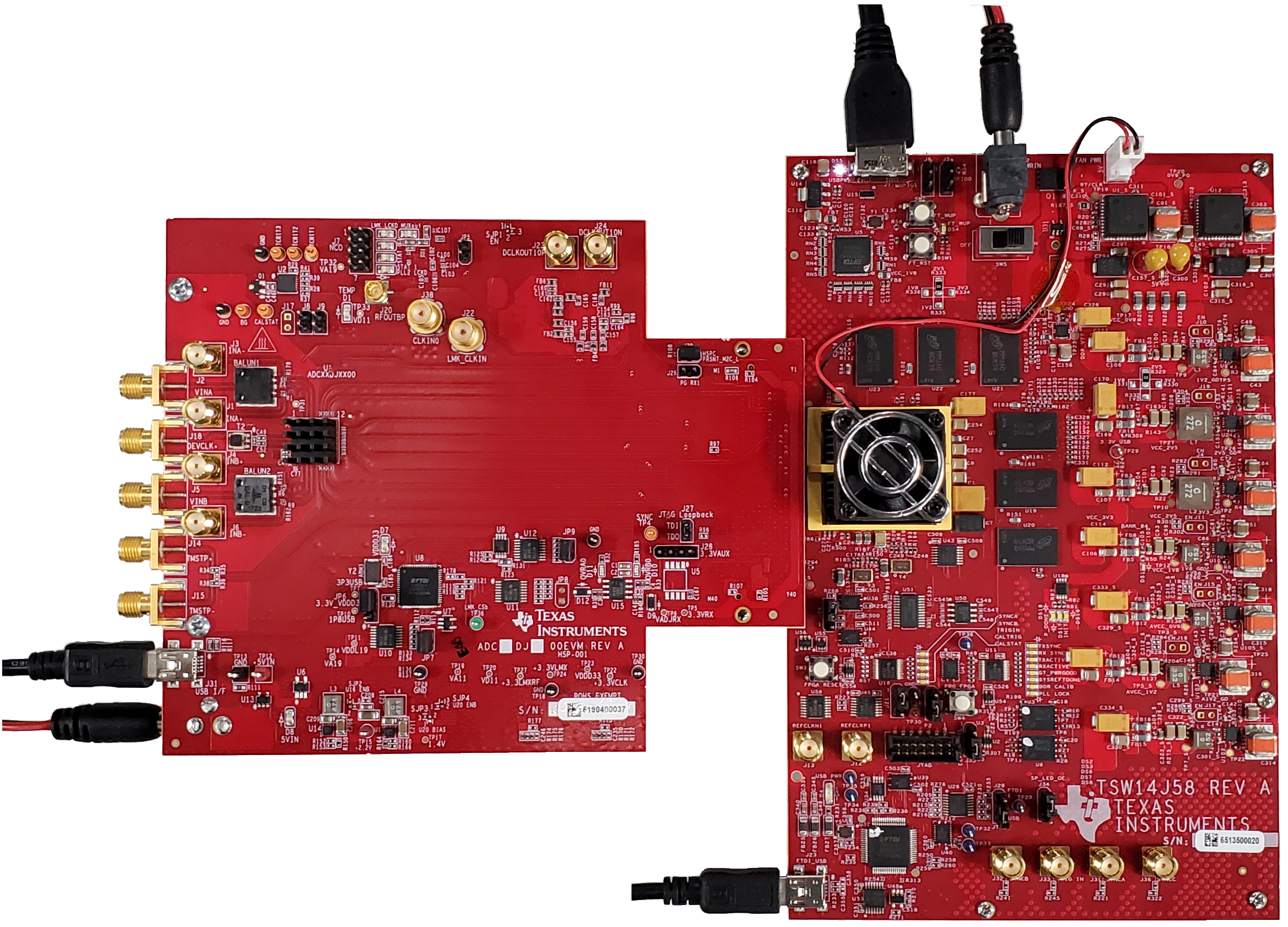
- Connect the ADC12DJ3200 EVM to the TSW14J58 EVM using the FMC connector.
- Provide +6 VDC connection to J2 of the TSW14J58 EVM and +5 VDC connection to J37 of the ADC12DJ3200 EVM.
- Connect a Micro-USB 3.0 cable to J1 and a Mini-USB 2.0 cable to J23 of the TSW14J58 EVM.
Connect a Mini-USB 2.0 cable to J31 of the ADC12DJ3200 EVM.
Power up the TSW14J58 and ADC12DJ3200 EVMs.
The TSW14J58 EVM connected to an ADC12DJ3200 EVM is shown in Figure 7-6.
 Figure 6-2 TSW14J58 EVM connected to an ADC12DJ3200 EVM
Single Tone FFT Test
- The evaluation of the ADC12DJ3200 EVM requires programming the ADC, LMK04828, and LMX2582 devices. This process is easy using the ADC12DJxx00EVM GUI.
- Open the ADC12DJ3200 GUI and connect to the ADC.
- Select the onboard clock as the clocking source and choose a sampling rate from the drop down menu. This example uses a 3Gsps sampling rate.
- Choose JMODE3 as the Decimation and Serial Data Mode (Dual channel, 16 JESD204B lanes).
- Press the Program Clocks and ADC button and wait for programming to complete.
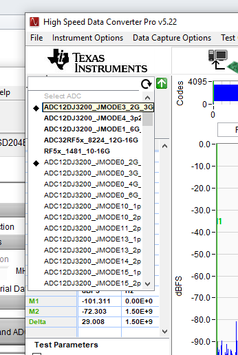
- Start the HSDC Pro GUI program. When the program starts, first connect to the TSW14J58 EVM board and then select the device ADC12DJ3200_JMODE3_2G_3G under the the Select ADC drop-down menu, as seen in Figure 7-7.
 Figure 6-3 Select ADC12DJ3200_JMODE3_2G_3G in the HSDC Pro GUI Program
 - When prompted by Load ADC Firmware?, select YES
- Select Single Tone FFT Test under Test Selection.
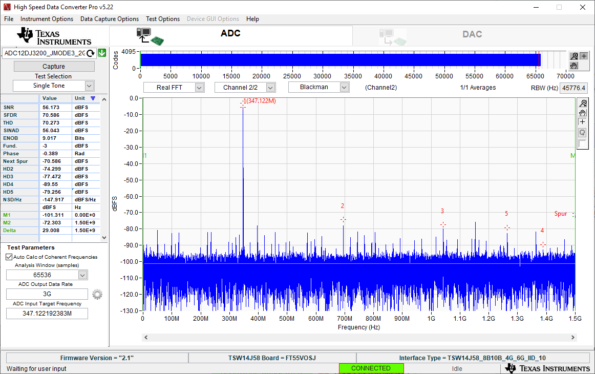
- Select the number of sample points (and resulting number of FFT bins) to be used. The example shown in Figure 7-8 has 65536 samples.
- Enter the ADC12DJ3200 sampling rate. The example shown in Figure 7-8 has the sample rate set at 3 Gsps.
- Enter the input frequency desired. The example shown in Figure 7-8 has the filtered input frequency set at 347 MHz and -3 dBFs on the HSDC Pro FFT plot.
- Select the channel the signal generator is connected to (channel B shown).
Press the Capture button on the HSDC Pro GUI.
Observe an FFT result similar to that of Figure 7-8.
 Figure 6-4 ADC12DJ3200 Operating in JMODE3 at 3 Gsps with 347-MHz Input Signal