SLYA042 July 2024 FDC1004 , FDC1004-Q1
- 1
- Abstract
- Trademarks
- 1 Introduction
- 2 CSAs and Input Bias Stage
- 3 CSA and Gain Error Factor
- 4 Applications for Resistance at Input Pins of Current Sense Amplifiers
- 5 Applications for Input Resistance at Reference Pins of Current Sense Amplifiers
- 6 Design Procedure and Error Calculation for External Input Resistance on CSA
- 7 Design Procedure for Input Resistance on Capacitively-Coupled Current Sense Amplifier
- 8 Design Procedure for Input Resistance at CSA Reference Pins
- 9 Input Resistance Error Test with INA185 Over Temperature
- 10Input Resistance Error Test with INA191 Over Temperature
- 11Derivation of VOS, EXT for a Single Stage Current Sense Amplifier (CSA)
- 12Summary
- 13References
4 Applications for Resistance at Input Pins of Current Sense Amplifiers
Table 4-1 is a non-comprehensive list of applications and reasons why a system needs resistors at the input pins (IN+ and IN-) for a current sense amplifier.
Table 4-1 Applications for Using Current
Sense Amplifier (CSA) with Input Resistors
| Application Type | Application Benefits |
|---|---|
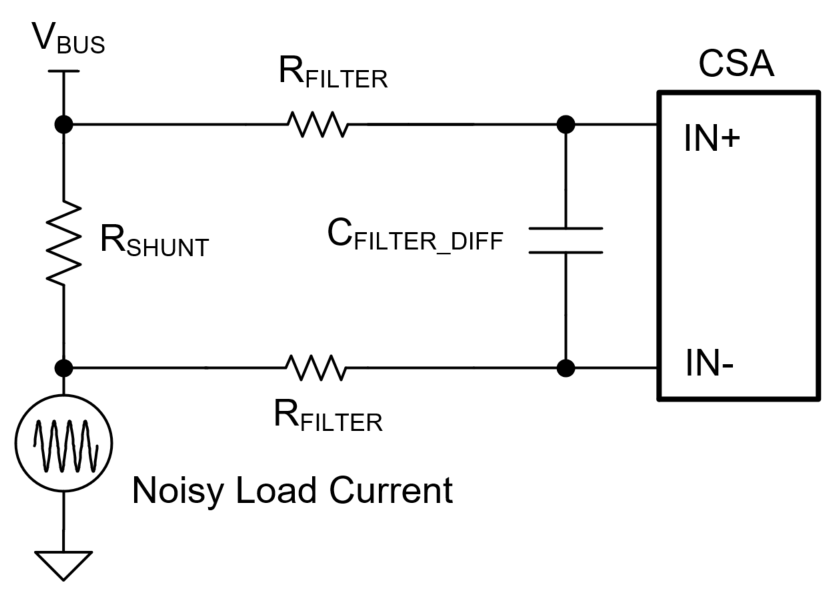
| Input differential (VSHUNT) filtering with input CDIFF capacitor as shown in Figure 4-1 |
|
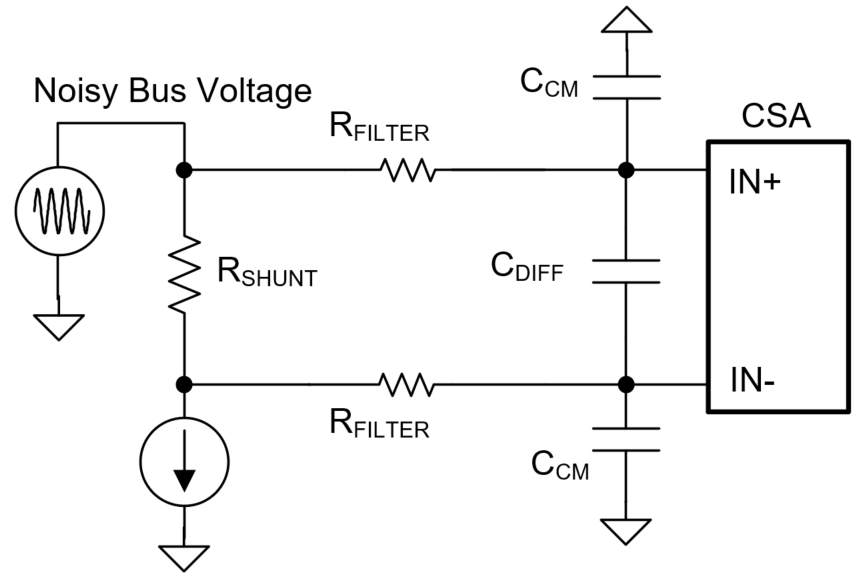
| Input common-mode voltage (VCM) filtering (with input CCM capacitors). See Figure 4-2. |
|
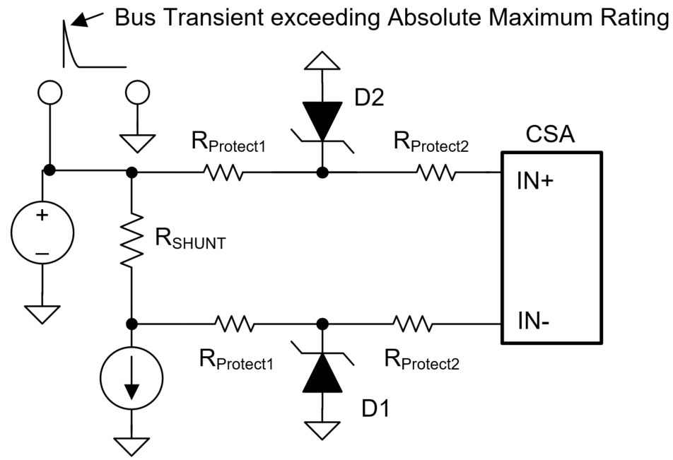
| Input current limiting for input VCM violation events: ESD fast-transient or DC electrical overstress (EOS). See Figure 4-3. |
|
For Figure 4-1, the input filter cutoff frequency is fC,differential = 1 / (2 × PI × 2 × RFILTER × CDIFF).
 Figure 4-1 Current Sense Amplifier with
Input Differential Filter
Figure 4-1 Current Sense Amplifier with
Input Differential FilterFor Figure 4-2, the input filter cutoff frequency is fC,differential = 1 / (2 × PI × 2 × RFILTER × (CDIFF + CCM / 2)).
 Figure 4-2 Current Sense Amplifier
With Input Common-Mode Filter
 Figure 4-3 Current Sense Amplifier
With Input Protection Diode Clamps and Resistors