SLYA042 July 2024 FDC1004 , FDC1004-Q1
- 1
- Abstract
- Trademarks
- 1 Introduction
- 2 CSAs and Input Bias Stage
- 3 CSA and Gain Error Factor
- 4 Applications for Resistance at Input Pins of Current Sense Amplifiers
- 5 Applications for Input Resistance at Reference Pins of Current Sense Amplifiers
- 6 Design Procedure and Error Calculation for External Input Resistance on CSA
- 7 Design Procedure for Input Resistance on Capacitively-Coupled Current Sense Amplifier
- 8 Design Procedure for Input Resistance at CSA Reference Pins
- 9 Input Resistance Error Test with INA185 Over Temperature
- 10Input Resistance Error Test with INA191 Over Temperature
- 11Derivation of VOS, EXT for a Single Stage Current Sense Amplifier (CSA)
- 12Summary
- 13References
3 CSA and Gain Error Factor
The typical device gain shown in data sheets for a single-stage, differential CSA is simply the matched ratio of RFB over RINT as shown in Equation 2.
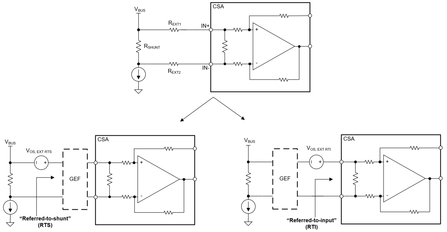
When using input resistors (REXTERNAL or REXT), the total shunt voltage gain (GainTOTAL) becomes predictably attenuated due to a Gain Error Factor (GEF) that is less than 1. This new attenuated gain can be theoretically calculated using Equation 3. This total shunt voltage gain is now the new typical gain of the circuit. Note equations for a device's GEF are usually provided in data sheet.
When introducing an input GEF, there is a new way to reference input offset voltages. Normally, the initial offset error specified in the data sheet (VOSI) is referred to the input (RTI), but to refer it to the shunt (RTS), you need to divide by the GEF. This also applies to the derivation of VOS, EXT RTI shown at end of document.
 Figure 3-1 RTI (Referred-to-input) and
RTS (Referred-to-shunt) for CSA with Input Resistors
Figure 3-1 RTI (Referred-to-input) and
RTS (Referred-to-shunt) for CSA with Input ResistorsOnce the new typical total gain is determined, the designer can shift (calibrate) the shunt voltage gain in system hardware or software. However, there can be a significant increase in gain error variation (EG, EXT) over system population due to the fact that internal resistors are designed to achieve accurate ratios (Device Gain = RFB/RINT), not accurate absolute values.
For most CSAs, conservative evaluations put the absolute process variation (PV) of these resistors at ±20% and with temperature coefficients (PV_TC) of ±30 ppm/°C. These are based upon the specifications of the process technology. Furthermore, error analysis is simplified by the fact that all internal resistors for a single device can inherently have the same PV and PV_TC. With these PV specifications defined, a designer can calculate the bounds of external resistance loading error (eEXT).