This application note discusses how the TMAG5328 resistor and voltage adjustable, low-power Hall-effect switch can increase system design flexibility and reduce design time. In addition, the document also discusses how using voltage to adjust the TMAG5328’s BOP enables multiple applications. One of these applications is a software programmable Hall-effect switch with microcontroller-less standalone mode, which is done by using a DAC or digital potentiometer with nonvolatile memory. Additionally, the document discusses how sweeping the voltage that sets the BOP can be used to back-calculate the sensed magnetic flux density seen by the TMAG5328. This document also discusses how adding a square wave voltage waveform can help the TMAG5328 implement diagnostics for detecting faults such as TMAG5328 device pin shorts, TMAG5328 device pin disconnections, and when a system’s magnet is either too close or too far from the sensor. The magnet out-of-range functionality implemented for diagnostics can also be reused as a magnetic window comparator instead.
All trademarks are the property of their respective owners.
Many systems require a mechanism to detect the mechanical position between a moving component in the system and a fixed component. Systems that only require a simple binary detection of position are often implemented by placing a magnet on the movable component and a Hall-effect switch on the fixed component (the base). An example of an open/close detection system is the mechanism in refrigerators that detect when the refrigerator’s door (the moving component) is open or closed, which determines when to turn ON or OFF the refrigerator light. In Figure 1-1, a magnet is placed on the moving refrigerator door and the Hall-effect switch is placed on a fixed PCB underneath the refrigerator base. In this example, it is assumed that the center of the magnet is directly above the sensing element of the Hall sensor when the refrigerator door is closed.
Figure 1-2 shows an example output graph of the TMAG5328 omnipolar Hall-effect switch. The device in Figure 1-2 is an omnipolar device, therefore the output responds to both positive and negative magnetic flux densities, which means the device responds the same regardless if the north or south pole of a magnet approaches the device. As the magnet approaches the Hall-effect switch, the magnitude of the sensed magnetic flux density increases. When the applied magnetic flux density exceeds the BOP threshold, the device in Figure 1-2 outputs a low voltage. The output of the device in Figure 1-2 stays low until the magnetic flux density decreases to less than BRP, and then the output drives a high voltage.
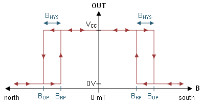
The relationship between the sensed magnetic flux density and the magnet-to-sensor distance along with the BOP and BRP determine the magnet-to-sensor distance at which the switch changes state. In many cases, the magnet travels in a direct linear path of travel, so distance is often expressed by the direct magnet-to-sensor distance. In Figure 1-1, however, distance is specified by the angle of opening because the refrigerator door opens on a hinge that causes the magnet to move nonlinearly. For Figure 1-1, the magnet-to-sensor distance increases as the angle of opening increases.
Figure 1-3 shows an example graph of how the sensed magnetic flux density varies as the angle of the opened refrigerator door 1 varies. The magnet-to-sensor distances at which the switch changes state depends on the BOP and BRP. If you want to determine the typical distance at which the sensor switches state, find the locations on the Figure 1-3 plot where the sensed magnetic flux density values are equal to the BOP,TYP and BRP,TYP specifications listed in the device data sheet. Alternatively, when determining the worst-case device to device variation for output switching, refer to the BOP,Max and BRP,Min specifications. BOP,Max and BRP,Min account for process variation, temperature and voltage. Designing the system within these bounds will result with consistent operation despite these variables.
As an example, let’s say there are two Hall-effect switches with the following specs:
Switch 1
BRP,MIN =5.12 mT
BRP,TYP =6.87 mT
BOP,TYP =7.87 mT
BOP,MAX =9.62 mT
Switch 2
BRP,MIN =0.73 mT
BRP,TYP =1.58 mT
BOP,TYP =2.58 mT
BOP,MAX =3.43 mT
If switch 1 is used in refrigerator 1, the output of switch 1 will be low when the angle of opening for door 1 is ≤1.8°, regardless of variations in process variation, temperature, and voltage. The angle of opening for door 1 is ≤1.8° when the sensed magnetic flux density is greater than the 9.62 mT BOP,MAX. However, the typical distance where the output of switch 1 is asserted low would be at 2°, which is when the sensed magnetic flux density equals the device’s BOP,TYP value of 7.87 mT. The output of switch 1 will be high when angle of opening for door 1 is ≥2.5°, which is when the sensed magnetic flux density is less than the 5.12 mT BRP,MIN. The typical distance where the output of switch 1 is asserted high, however, would be at 2.2°.
If switch 2 is used in refrigerator 2, the typical distance at which the output of switch 2 is asserted low would be at 3.5°. The output would be low at an angle ≤3.1° regardless of variations in process variation, temperature, and voltage. Additionally, the output of switch 2 would be asserted high at 4.4° typically. The output would be asserted high at an angle ≥6.0° regardless of variations. The different switching distances of switches 1 and 2 shows how switching distance is dependent on the BOP and BRP specs of a Hall sensor.
Most Hall-effect switches have a fixed BOP, which typically imposes design constraints on the placement and specifications of the magnet needed to ensure switching of the Hall-effect sensor at the desired distance. To allow design flexibility, many Hall-effect switches come with multiple device variants with different BOP values; however, there are only a finite number of BOP options available with a Hall-effect switch, which still puts constraints on the placement and specifications of the magnet.
The TMAG5328 Hall-effect switch, on the other hand, has an adjustable BOP that can be programmed anywhere between 2 to 15 mT by applying a voltage or connecting a resistor to the ADJ pin of the device. By following simple formulas, it is easy to calculate what resistor value or voltage value is needed to set up the right BOP value. The hysteresis value of the TMAG5328 is fixed to 1 mT, which results in the BRP value being BOP – 1 mT. As an example, if the BOP is set to 5 mT, the BRP would be set to 4 mT.
To set the BOP of the TMAG5328 using an external resistor, connect the resistor between the ADJ and GND pins of the device. Figure 1-4 shows the relationship between BOP and resistance defined as BOP(mT) = RADJ(kΩ). The BOP of the TMAG5328 must be set to a value between 2 mT and 15 mT, RADJ must be set between 2 kΩ and 15 kΩ.
The other method to setup the BOP is to apply a voltage to the ADJ pin. The relationship between BOP and voltage is defined as BOP(mT)= VADJ(mV) × 0.0125. To apply a voltage on the ADJ pin, the voltage source must be able to settle within 4 µs after being exposed to a 80-µA current on the ADJ pin. Figure 1-5 shows that the TMAG5328 BOP must be set to a value between 2 mT and 15 mT and the VADJ must be set between 160 mV and 1200 mV.
The adjustable BOP of the TMAG5328 enables design flexibility that fixed BOP Hall-effect switches cannot provide. The advantages of the TMAG5328 programmable BOP include the following:
To estimate the magnetic flux density sensed by the TMAG5328, connect a DAC or other voltage source to the TMAG5328 ADJ pin and follow the procedure below:
The more DAC steps there are between the 0.16 V to 1.2 V VADJ operating range of the TMAG5328 and the higher the DAC accuracy, the more accurate the estimate of the sensed magnetic flux density. However, using more DAC steps results in a longer execution time for estimating the sensed magnetic flux density. In the TMAG5328EVM, the DAC43701 DAC is used to determine the magnetic flux density sensed by the TMAG5328. The DAC43701 is an 8-bit DAC that is configured to use a 0 V to 1.82 V range. From this 0 V to 1.82 V range, 144 of the possible 256 DAC codes can be used with the TMAG5328 because these codes fall within the 0.16 V to 1.2 V VADJ range of the TMAG5328. The DAC43701 is pin-to-pin compatible with the 10-bit DAC53701, therefore the DAC53701 can replace the DAC43701 on the EVM to allow 584 usable codes within the 0.16 V to 1.2 V VADJ range of the TMAG5328. Using the DAC53701 can enable a slightly more precise estimate of the sensed magnetic flux density than the DAC43701; however, the more codes that are used for determining the sensed magnetic flux density, the longer it takes for the procedure to run. If 100 ms is spent at each DAC code between the 0.16 V to 1.2 V VADJ range of the TMAG5328, it would take about 14.4 seconds to iterate through all the DAC43701 codes and 58.4 seconds to iterate through all the DAC53701 codes.
Figure 2-1 shows a logic analyzer screenshot when this procedure was conducted using the TMAG5328 and DAC43701 devices on the TMAG5328EVM. In Figure 2-1, the Timer ISR plot shows a pulse every time the DAC output changes, the TMAG5328 OUTPUT plot shows the state of the TMAG5328 OUT pin across time, and the DAC Output Voltage plot measures the DAC output voltage across time. In Figure 2-1, the output is asserted low at VDAC = 0.702 V, which indicates that the sensed magnetic flux density is approximately 8.78 mT. The time it takes for this procedure to run depends on how large the sensed magnetic flux density is, where larger magnetic flux densities result in shorter execution times. In the example below, the procedure completed in about 6 to 7 seconds.
The TMAG5328 can be made into a software-programmable Hall-effect switch by connecting a software-programmable voltage source with nonvolatile memory to the TMAG5328 ADJ pin. The voltage source could be a DAC or digital potentiometer. Figure 3-1 shows the TMAG5328EVM which specifically uses the DAC43701 8-bit DAC with nonvolatile memory to turn the TMAG5328 into a software-programmable Hall-effect switch. The devices are nearly pin-to-pin compatible, therefore the DAC43701 DAC can be replaced with the higher-resolution DAC53701 DAC or the TPL1401 digital potentiometer (DPOT).
The nonvolatile memory on these DAC/DPOT devices can be programmed to initialize the device to a user-defined output voltage every time the system is powered ON or when another type of RESET event occurs. The output of the DACx3701 or TPL1401 drives the ADJ pin of the TMAG5328, therefore the TMAG5328 BOP will also be automatically programmed after the system is powered ON. A microcontroller, which on the EVM is on a second PCB called the Sensor Controller Board (SCB), is only necessary to initially program the DAC nonvolatile memory. After the DAC nonvolatile memory is programmed to automatically output a voltage to create the user-defined BOP, the microcontroller is no longer needed. Only the DAC/DPOT and TMAG5328 devices are needed to ensure that the BOP settings are maintained.
In-system calibration can also be supported by following the procedure below:
In-system calibration allows the user to obtain their desired system functionality when magnet placement or manufacturing tolerance can vary greatly from device to device.
Instead of relying on applying a specific condition on the VCC pins of a device, this calibration scheme uses the DAC I2C interface to program the switch, which makes it easier to program. This approach does not require an additional power supply circuit to program the Hall-effect switch. The I2C interface of the DAC allows software-based modification of the BOP, which can enable in-field upgrades of an already deployed unit without performing hardware modification. In addition, four DAC43701 devices can be put on the same I2C bus. If the programming micrcocontroller has multiple I2C interfaces, then more than four systems can be programmed at the same time, thereby further reducing the time needed to perform mass calibration.
The TMAG5328EVM supports this in-system calibration technique. The TMAG5328EVM’s Quick Start Video shows an example of this in-system calibration technique by using the head-on linear displacement 3D print attachment.
A square wave voltage waveform on the ADJ pin of the TMAG5328 can help a user detect under certain conditions when the TMAG5328 pins have been disconnected or shorted to other pins. This technique for implementing diagnostics works by applying a square wave on the TMAG5328 ADJ pin, which allows the pin to alternate the BOP and BRP of the TMAG5328 in a way to also create a square wave output on the TMAG5328 OUT pin. You can use a DAC to create the square wave, or you can use another voltage output circuit to create a voltage waveform that alternates between two voltages somewhere within the 0.16 V and 1.2 V. During the diagnostic check, a microcontroller can check to confirm the TMAG5328 OUT pin changed state after the ADJ pin square wave changed state. If the TMAG5328 OUT pin does not change state after the ADJ square wave changes state, a fault may have occurred.
The high and low voltage values of the square wave create two BOP values that alternated between. When the high voltage of the square wave is applied to the ADJ pin, it creates a larger BOP, which is referred to as BOP,HIGH. It also results in a new BRP, which is referred to as BRP,HIGH. If the sensed magnetic flux density in the system (BSystem) is less than BRP,HIGH, the TMAG5328 output is asserted high when the high portion of the square wave is applied to the ADJ pin. When the low voltage of the square wave is applied to the ADJ pin, it creates a smaller BOP, which is referred to as BOP,LOW. If BSystem is greater than BOP,LOW, the TMAG5328 output is asserted low when the low portion of the square wave is applied to the ADJ pin. Consequently, the produced square wave on the TMAG5328 output should change state after the square wave on its ADJ pin switches from high to low or low to high.
In addition to detecting signal shorts and disconnections, this technique also implements a magnetic window comparator that detects when the sensed magnetic flux density is either greater than BOP,HIGH or less than BRP,LOW. If the high voltage value of the square wave is selected so that BRP,HIGH is larger than the maximum magnetic flux density reading expected in the system and the low voltage of the square wave is selected so that BOP,LOW is less than the minimum magnetic flux density reading expected in the system, the window comparator can potentially detect when there is a fault due to the system’s magnet being either too close or too far from its normal range of positions.
For this diagnostic technique to properly function, you must meet the following constraints:
BOP,LOW ≥ 2 mT (this means that the low output voltage of the square wave must be ≥ 0.16 V)
BOP,HIGH ≤ 15 mT (this means that the high output voltage of the square wave must be ≤ 1.2 V)
BOP,LOW ≤ BSystem (this is needed to ensure that the TMAG5328 output is asserted low when the low portion of the square wave is applied)
BSystem ≤ BRP,HIGH (this is needed to ensure that the TMAG5328 output is asserted high when the high portion of the square wave is applied)
The square wave pulse width duration, referred to as tOP, must be greater than the TMAG5328 period of magnetic sampling. This requirement ensures that the TMAG5328 has enough time to update its BOP based on the voltage provided to the ADJ pin. For example, as the TMAG5328 period of magnetic sampling is 50 ms, using a value of tOP = 100 ms is more than sufficient to meet this requirement.
Figure 4-1 shows a visual representation of these constraints.
This diagnostic technique was tested on the TMAG5328EVM by loading firmware on the EVM's microcontroller that would generate a timer interrupt every 100 ms. In the firmware, the DAC produces a square wave that alternates between 0.68 V (the low state) and 1.04 V (the high state), which creates a BRP,HIGH value of 12 mT and a BOP,LOW value of 8.5 mT. The head-on linear displacement attachment was connected to the TMAG5328 and configured so that the TMAG5328 sees a magnetic field between 8.5 mT to 12 mT.
In the timer interrupt service routine, the TMAG5328 output is first read. If the DAC output voltage is at 1.04 V, the TMAG5328 OUT pin should be high. If the DAC output voltage is currently at 0.68 V, the TMAG5328 OUT pin should be low. If the TMAG5328 OUT pin is not in the correct state, a fault has occurred, which is logged by the microcontroller.
After checking the state of the TMAG5328 OUT pin, the microcontroller configures the DAC to switch to 1.04 V if the TMAG5328 OUT pin is currently at 0.68 V or switch to 0.68 V if the TMAG5328 OUT is currently at 1.04 V. The TMAG5328 output is checked at the next timer interrupt, which gives the TMAG5328 enough time to update its BOP.
Figure 4-2 below shows the expected waveform on the TMAG5328 OUT pin when no faults are present. Due to the OUT pin changing states, the LED connected to the TMAG5328EVM would blink at a frequency equal to the frequency of the DAC square wave (approximately 5 Hz).
The out-of-range test provides an alert when the observed magnetic flux density is outside the system’s range of expected magnetic flux density readings. Out-of-range fault detection was specifically tested on the TMAG5328EVM by adjusting the position of the inner screw of the head-on linear displacement 3D print, as shown in Figure 4-3.
In its initial state, the inner screw of the attachment, which has an embedded magnet, was placed so that the sensed magnetic flux density of the TMAG5328 was between 8.5 mT to 12 mT. The inner screw of the 3D print was screwed into the outer base until the sensed magnetic flux density was greater than 12 mT. Figure 4-3 shows the resulting logic analyzer screenshot, which shows that the TMAG5328 OUT pin is asserted low even when the DAC is in the high state. A square wave is no longer present on the TMAG5328 OUT pin, which means this diagnostic technique detected when the magnetic flux density was greater than 12 mT due to the magnet being too close. This scenario was also correctly logged by the EVM’s microcontroller as a fault condition.
Next, the inner screw of the 3D print was unscrewed until the sensed magnetic flux density was back to being between 8.5 mT to 12 mT, which resulted in a square wave appearing onto the TMAG5328 OUT pin again like it was in Figure 4-2. The inner screw was further unscrewed until the sensed magnetic flux density was less than 8.5 mT. Figure 4-5 shows the resulting logic analyzer screenshot from the sensed magnetic flux density being less than 8.5 mT. Figure 4-5 shows that the TMAG5328 OUT pin is asserted high even when the DAC is in the low state. A square wave is no longer present on the TMAG5328 OUT pin, which means this diagnostic technique detected when the magnetic flux density was less than 8.5 mT due to the magnet being too far or no longer present in the system. Additionally, the microcontroller was able to correctly to log this as a fault event.
This out-of-range test can also potentially detect if there is an external magnetic field present in the system that is causing the TMAG5328 device to see a magnetic flux density reading it should not normally observe.
After conducting the out-of-range test, the screw component of the 3D print was screwed back into the base so that the magnetic flux density was between 8.5 mT to 12 mT again so that the other faults can be detected.
This diagnostic technique was also tested by disconnecting the TMAG5328 ADJ pin from the DAC, disconnecting the TMAG5328 VCC pin from the power supply, and disconnecting the TMAG5328 OUT pin from the OUT signal probed by the logic analyzer and microcontroller.
When the ADJ pin was disconnected from the DAC, the output of the TMAG5328 was either asserted low (Figure 4-6) or high (Figure 4-7). In both cases, the TMAG5328 OUT pin did not have a square wave with frequency equal to the DAC voltage frequency, which would indicate that a fault occurred.
When VCC was disconnected from the TMAG5328, the OUT pin was observed low, as shown in Figure 4-8. This was logged by the EVM’s microcontroller as a fault event.
Similarly, the OUT pin was also observed low when the TMAG5328 OUT pin was disconnected, as shown in Figure 4-9. As a result of the OUT pin being stuck low, the EVM’s microcontroller also logged this as a fault event.
The TMAG5328 OUT pin did not have a square wave after VCC or OUT were disconnected, therefore this technique was able to detect these signal disconnection faults.
This diagnostic implementation was tested when the TMAG5328 OUT pin was shorted to GND and shorted to VCC. When the TMAG5328 OUT pin was shorted to GND, the OUT pin stayed low, as shown in Figure 4-10. Shorting the TMAG5328 OUT pin to VCC caused the OUT pin to stay high, as shown in Figure 4-11. For both signal shorts, a square wave was no longer available on the TMAG5328 OUT pin, so the EVM’s microcontroller was able to log these events as faults.
By connecting the TMAG5328 to a DAC with nonvolatile memory, a software programmable Hall-effect switch with microcontroller-less standalone mode can be implemented. Using a DAC also enables backcalculating the magnetic flux density seen by the device. In addition, the DAC can be configured to implement diagnostics on the TMAG5328 to detect TMAG5328 pin shorts, TMAG5328 pin disconnections, and magnet out of range faults. These applications as well as the other applications of the TMAG5328 adjustable BOP increases system design flexibility and reduces design time.
TI PROVIDES TECHNICAL AND RELIABILITY DATA (INCLUDING DATASHEETS), DESIGN RESOURCES (INCLUDING REFERENCE DESIGNS), APPLICATION OR OTHER DESIGN ADVICE, WEB TOOLS, SAFETY INFORMATION, AND OTHER RESOURCES “AS IS” AND WITH ALL FAULTS, AND DISCLAIMS ALL WARRANTIES, EXPRESS AND IMPLIED, INCLUDING WITHOUT LIMITATION ANY IMPLIED WARRANTIES OF MERCHANTABILITY, FITNESS FOR A PARTICULAR PURPOSE OR NON-INFRINGEMENT OF THIRD PARTY INTELLECTUAL PROPERTY RIGHTS.
These resources are intended for skilled developers designing with TI products. You are solely responsible for (1) selecting the appropriate TI products for your application, (2) designing, validating and testing your application, and (3) ensuring your application meets applicable standards, and any other safety, security, or other requirements. These resources are subject to change without notice. TI grants you permission to use these resources only for development of an application that uses the TI products described in the resource. Other reproduction and display of these resources is prohibited. No license is granted to any other TI intellectual property right or to any third party intellectual property right. TI disclaims responsibility for, and you will fully indemnify TI and its representatives against, any claims, damages, costs, losses, and liabilities arising out of your use of these resources.
TI’s products are provided subject to TI’s Terms of Sale (www.ti.com/legal/termsofsale.html) or other applicable terms available either on ti.com or provided in conjunction with such TI products. TI’s provision of these resources does not expand or otherwise alter TI’s applicable warranties or warranty disclaimers for TI products.
Mailing Address: Texas Instruments, Post Office Box 655303, Dallas, Texas 75265
Copyright © 2022, Texas Instruments Incorporated