SLYS018F April   2018  – October 2024 INA181-Q1 , INA2181-Q1 , INA4181-Q1

PRODUCTION DATA  

  1.   1
  2. Features
  3. Applications
  4. Description
  5. Device Comparison
  6. Pin Configuration and Functions
  7. Specifications
    1. 6.1 Absolute Maximum Ratings
    2. 6.2 ESD Ratings
    3. 6.3 Recommended Operating Conditions
    4. 6.4 Thermal Information
    5. 6.5 Electrical Characteristics
    6. 6.6 Typical Characteristics
  8. Detailed Description
    1. 7.1 Overview
    2. 7.2 Functional Block Diagrams
    3. 7.3 Feature Description
      1. 7.3.1 High Bandwidth and Slew Rate
      2. 7.3.2 Bidirectional Current Monitoring
      3. 7.3.3 Wide Input Common-Mode Voltage Range
      4. 7.3.4 Precise Low-Side Current Sensing
      5. 7.3.5 Rail-to-Rail Output Swing
    4. 7.4 Device Functional Modes
      1. 7.4.1 Normal Mode
      2. 7.4.2 Unidirectional Mode
      3. 7.4.3 Bidirectional Mode
      4. 7.4.4 Input Differential Overload
      5. 7.4.5 Shutdown Mode
  9. Application and Implementation
    1. 8.1 Application Information
      1. 8.1.1 Basic Connections
      2. 8.1.2 RSENSE and Device Gain Selection
      3. 8.1.3 Signal Filtering
      4. 8.1.4 Summing Multiple Currents
      5. 8.1.5 Detecting Leakage Currents
    2. 8.2 Typical Application
      1. 8.2.1 Design Requirements
      2. 8.2.2 Detailed Design Procedure
      3. 8.2.3 Application Curve
    3. 8.3 Power Supply Recommendations
      1. 8.3.1 Common-Mode Transients Greater Than 26 V
    4. 8.4 Layout
      1. 8.4.1 Layout Guidelines
      2. 8.4.2 Layout Example
  10. Device and Documentation Support
    1. 9.1 Device Support
      1. 9.1.1 Development Support
    2. 9.2 Documentation Support
      1. 9.2.1 Related Documentation
    3. 9.3 Receiving Notification of Documentation Updates
    4. 9.4 Support Resources
    5. 9.5 Trademarks
    6. 9.6 Electrostatic Discharge Caution
    7. 9.7 Glossary
  11. 10Revision History
  12. 11Mechanical, Packaging, and Orderable Information

Application Curve

An example output response of a bidirectional configuration is shown in Figure 8-8. With the REF pin connected to a reference voltage (2.5 V in this case), the output voltage is biased upwards by this reference level. The output rises above the reference voltage for positive differential input signals, and falls below the reference voltage for negative differential input signals.
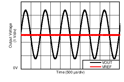
INA181-Q1 INA2181-Q1 INA4181-Q1 Bidirectional Application Output ResponseFigure 8-8 Bidirectional Application Output Response