SLYT835 March 2023
3 Active clamp leg design considerations
With the active snubber implemented in a PSFB, the transformer winding current will no longer rise monotonically during the effective duty cycle (Deff) period (TS) (non-zero output winding voltage period) like output inductor current. This is because the active snubber capacitor energy also participates in energizing output inductor rather than solely rely on energy transfer from the input side. The non-monotonic current ramp characteristic could make peak current mode control difficult as input or transformer winding current are generally utilized for peak current detection and higher input or transformer winding current does not necessarily represent larger duty cycle.
In order to allow peak current detection happens when current is rising monotonically, we must ensure DeffTS is always greater than the duration where current-second balance is completed – DCSBTS – under whole operational voltage and load ranges. As high efficiency is expected for a PSFB with larger Deff, PSFB is generally designed to have larger Deff at mid-to-heavy load where Deff >> DCSB is expected. At light load, converter is expected to operate under discontinuous conduction mode where Deff will be smaller than Deff under continuous conduction mode at the same input/output voltage condition. In order to keep DeffTS greater than DCSBTS even at light load, we have implemented frequency reduction control based on load current.
The duration of DCSBTS becomes an important factor for peak current mode control. How long does it take to complete current-second balance is now the one-million-dollar question. To answer this question, you’ll need to calculate current flow through the active clamp leg.
Assuming that VCL is a constant and Lm = ∞, Equation 2 expresses the rectifier current changing rate during the duty-cycle loss period (the period where VSEC = 0 and iSR1 and iSR2 are commuting) as:
where VLr is the voltage across Lr.
Equation 3 calculates the changing rate of the output inductor current:
Using Equation 2 and Equation 3 along with Kirchhoff’s current law, Equation 4 calculates the changing rate of the active clamp current:
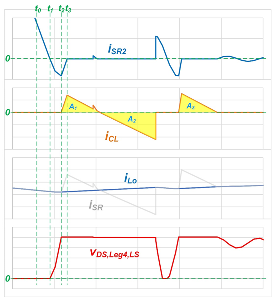
Since VCL ≈ VIN x NS/NP [3], you just need to apply the total active clamp leg conduction time as Δt in Equation 4 to solve ΔiCL. However, you still need to know the peak value of iCL in order to calculate the iCL root-mean-square (RMS) value. As shown in Figure 3-1, if iSEC = iLo (after charging Coss to VCL) at time t2 and iSEC = iSR at time t3 (start to charge CCL), Equation 5 derives iCL,peak as:
 Figure 3-1 Key waveforms around the
active clamp current conduction period.
Figure 3-1 Key waveforms around the
active clamp current conduction period.With Equation 6 deriving the iSR2 value at t2 as:
Assuming that the iSR2 current decreasing rate from t0 to t2 is the same, Equation 7 derives the time duration of t2-t1 as:
Since CLneeds to maintain a current second balance, the sum of areas A1 and A3 will equal area A2.
As shown in Equation 7, SR Coss controls the peak current on the active clamp leg. If you select a low Coss SR FET, the active clamp leg RMS current is lower and thus helps improve converter efficiency.
Here are some design guidelines when designing a PSFB converter with an active snubber:
- QCL must turn on only after the duty-cycle loss duration in order to avoid CCL energy backflow to the primary side.
- QCL must be turn on while the body diode is still conducting current for ZVS.
- A longer QCL on time will reduce VCL as well as SR voltage stress, but the QCL RMS current will increase.
- A lower SR Coss will not only help reduce the active clamp leg RMS current, but also help reduce SR voltage stress.
The active clamp method isn’t limited to full-bridge rectifiers; it is applicable to other types of rectifiers such as current-doubler [4] or center-taped rectifiers. Figure 3-2 shows a PSFB converter with an active clamp on a center-taped rectifier, which is implemented in the 3-kW Phase-Shifted Full Bridge with Active Clamp Reference Design with >270-W/in3 Power Density.
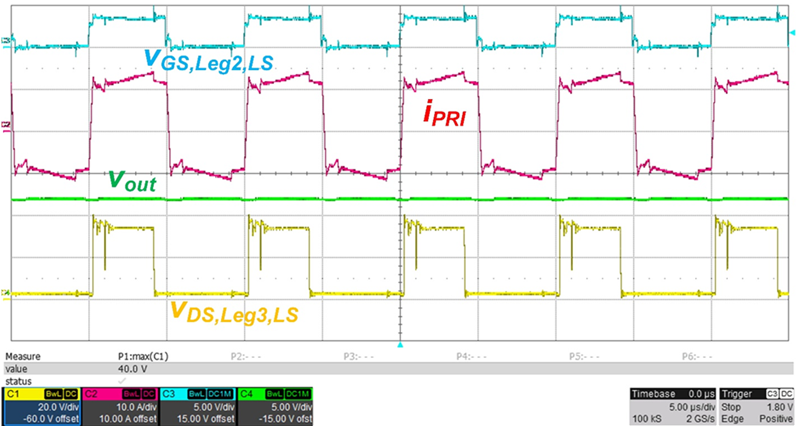
As shown in Figure 3-3, it is possible to clamp SR voltage stress under 40 V with dual active clamp legs, with negligible clamping loss (very minor conduction loss) at a 250-A load current.
 Figure 3-3 Steady-state waveform of a
PSFB converter with a center-taped rectifier and active snubbers at a 12-V/3-kW
output.