SLYT837 January 2023 TPS543B22 , TPS548A28 , TPS56121
4 Voltage-mode control architecture
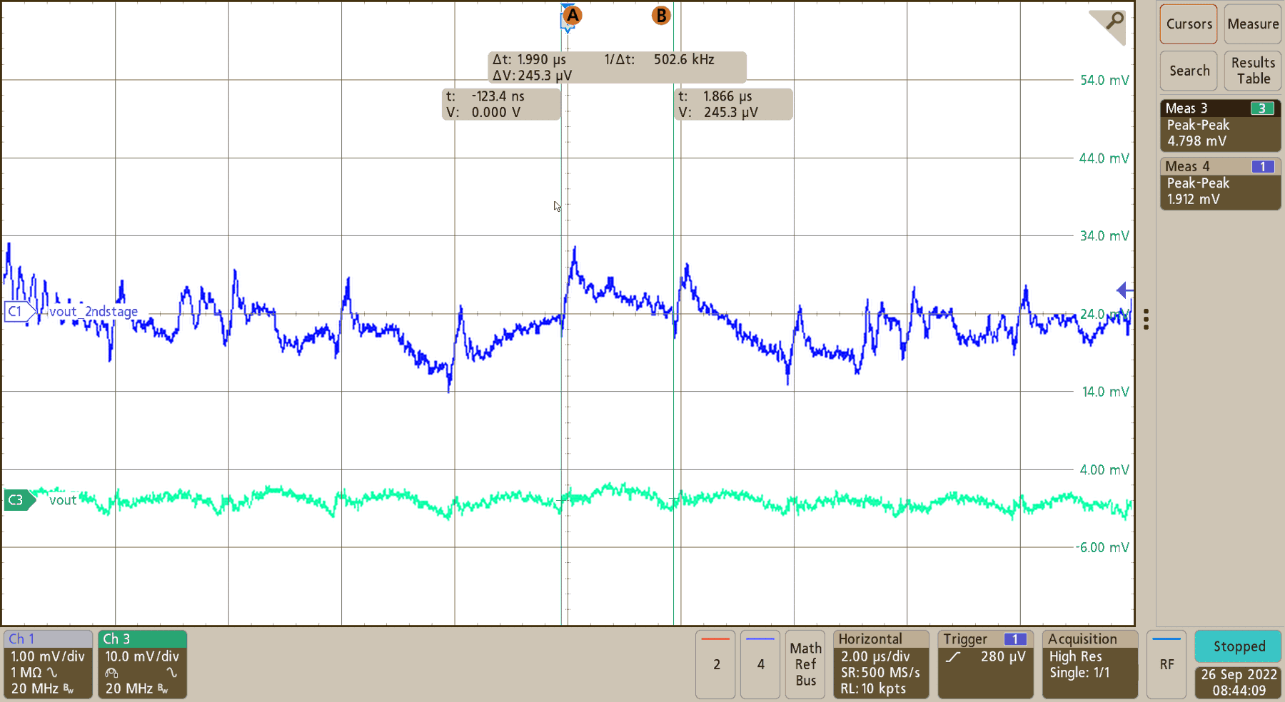
Pulse-width modulation (PWM) with voltage-mode control architecture is accomplished by comparing a voltage error signal from the output voltage and reference voltage to a constant sawtooth-ramp waveform. The ramp is initiated by a clock signal from an oscillator. The TPS56121 employs externally-compensated, type-3 compensation addressing a double-pole power stage that allows the converter to be re-compensated after the addition of a second-stage filter. Adjusting external resistor and capacitor values after the addition of a second stage filter ensures stability. The output voltage peak-to-peak ripple without an additional filter is 4.8-mV. With the additional filter applied, the output voltage ripple is 1.9-mV (as shown in Figure 4-1). In this case, the TPS56121 design required no loop compensation adjustments to ensure stability. Figure 4-2 shows a load transient waveform with a 10-A load-step, and the output voltage waveform after the implementation of the second-stage filter shows no sign of instability.
 Figure 4-1 TPS56121 output voltage ripple
with and without additional second-stage filter.
 Figure 4-2 Transient response of TPS56121
using voltage-mode control.