SLYT855 May 2024 AFE88101 , DAC161S997 , DAC8551 , TVS3301
- 1
- 1Introduction
- 2What is a solar power optimizer?
- 3Output bypass function of a solar power optimizer
- 4Output bypass circuit solutions
- 5A scalable bypass switch solution using a low-voltage ideal diode controller
- 6Working principle of LM74610-Q1 reverse-voltage range extension
- 7Conclusion
- 8Additional resources
6 Working principle of LM74610-Q1 reverse-voltage range extension
Depletion-mode MOSFETs are by default on when MOSFET VGS is 0V, unlike enhanced-mode MOSFETs that require VGS to be greater than the threshold voltage of the MOSFET. In order to turn off the depletion MOSFET, VGS needs to be <0V (typical ranges are from –1V to –4V). To analyze the effect of the depletion-mode MOSFET in an ideal diode-sense path, let’s look at device operation under these conditions:
- When VPV– VPV+: The ideal diode controller is in forward-condition mode, keeping both the power MOSFET Q1 and depletion FET QD on. With these operating conditions, you can calculate the output voltage as VOUT = VIN – (ID_Q1 RDS(on)_Q1), approximated to VPV+.
- When VPV– < VPV+: The ideal diode controller is in the reverse current blocking condition, with MOSFET Q1 turned off. MOSFET QD is in regulation mode as a source follower, maintaining VCATHODE above VANODE, VCATHODE = VIN(VANODE)+ (VGSMAX). So the voltage across VCATHODE to VANODE is within the absolute maximum rating VGSMAX of QD (usually <5V), which is far less than the maximum reverse voltage of 45V transient of the LM74610-Q1. The high reverse voltage (VOUT – VIN) is sustained by the drain-to-source voltage (VDS) of QD and Q1.
Selecting the correct depletion MOSFET and power MOSFET depends on these points:
- Choose a VDS rating of Q1 and QD greater than the maximum peak input voltage.
- Select RDS(on) such that dissipation across the power-path MOSFET is lowest. The drain current (ID) of the FET should be higher than the maximum peak current demanded by the output load. Selecting a depletion MOSFET with a drop of 50mV to 100mV across the power MOSFET at the full load current is a good starting point.
- RDS(on) can be in the hundreds of ohms range (the LM74610-Q1’s floating gate-drive architecture has a large impedance of cathode pin to ground, and the ICATHODE of the controller is in the microamperes range).
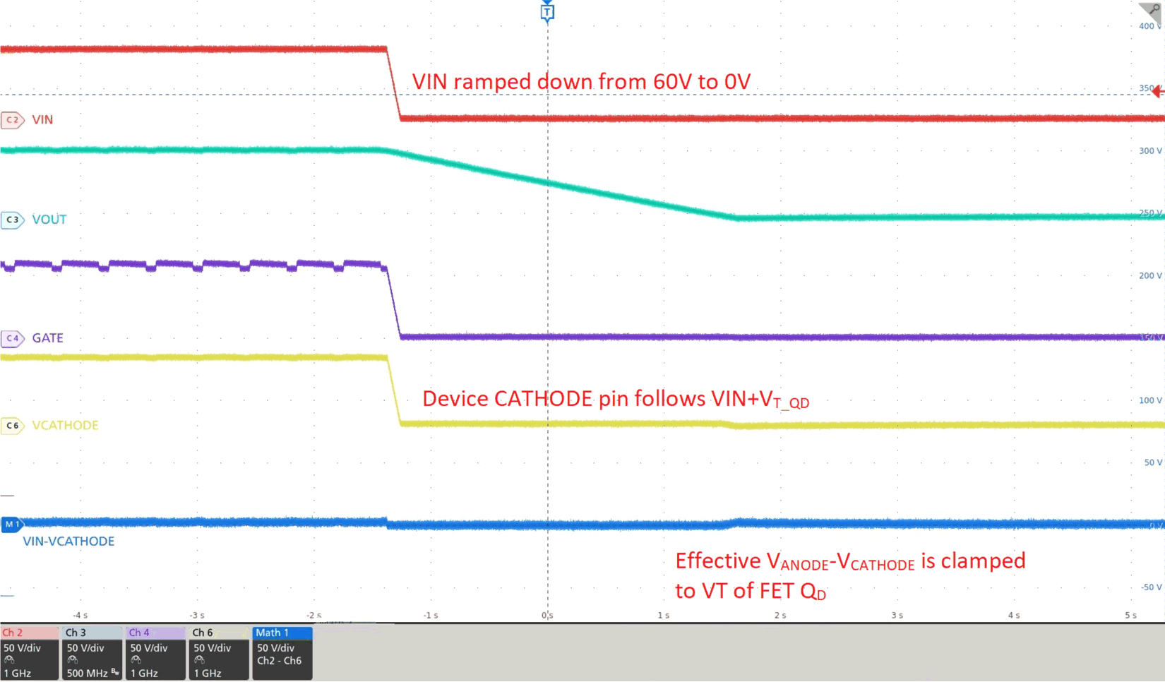
Figure 5 shows test results for a 60V bypass switch solution using the 40V LM74610-Q1 controller.
 Figure 5 Test results for a 60V bypass
circuit with the LM74610-Q1 and depletion MOSFET.
Figure 5 Test results for a 60V bypass
circuit with the LM74610-Q1 and depletion MOSFET.With properly scaled MOSFETs (Q1 and QD), the input voltage range can extend to the VDS rating of the FETs. This enables high-voltage designs using the same low-voltage controller. Also, extending the input voltage range can also be useful in enterprise, communication, power tool and high-voltage battery-management applications.