SLYU058D May 2021 – February 2024 TMAG5173-Q1 , TMAG5273
4.4 Direct EVM Serial Communication
If desired, the SCB can communicate directly with the EVM without the use of the GUI through the USB serial (COM) port. Simply send the desired command string over the serial port and receive the results. This is useful for interfacing the EVM with custom setups/scripts/GUIs. Note that the TMAG5x73EVM must be connected to the SCB to receive any command responses from the SCB.
To read and write registers, follow the below format:
- Read register command format: rreg ADR
- Where ADR is the address in hex, and rreg is always lower case
- Register addresses can be
in upper or lower case, and do not need to be led by "0x". 0 padding
register addresses is also optional. For example, to read register
address 0xE, some valid commands include:
- rreg e
- rreg 0E
- rreg 0x0E
- When "0x" is used, the "x" must be lower case.
- Figure 4-18 is an example response to this command:
 Figure 4-18 Example Register Read
Response
Figure 4-18 Example Register Read
ResponseThe number to the right of value represents the value read from the register. Note that this value is represented in decimal form and not hexadecimal.
- Write register command format: wreg ADR VAL
- Where ADR and VAL are in hex, and wreg is always lower case
- Register addresses and
values can be in upper or lower case, and do not need to be led by "0x".
0 padding register addresses and values is also optional. For example,
to write register address 0x0 with the value 4, some valid commands
include:
- wreg 0 4
- wreg 00 0x4
- wreg 0x00 0x04
- When "0x" is used, the "x" must be lower case.
- Figure 4-19 is an example response to this command:
 Figure 4-19 Example
Register Write Response
Other useful commands include the following:
- Firmware revision command format: id
- This command prints the EVM the SCB is configured for (TMAG5273EVM in this case) and the date associated with the version of the firmware loaded on the SCB.
- Figure 4-20 is an example response to this command:
 Figure 4-20 Example
Firmware Revision Command Response
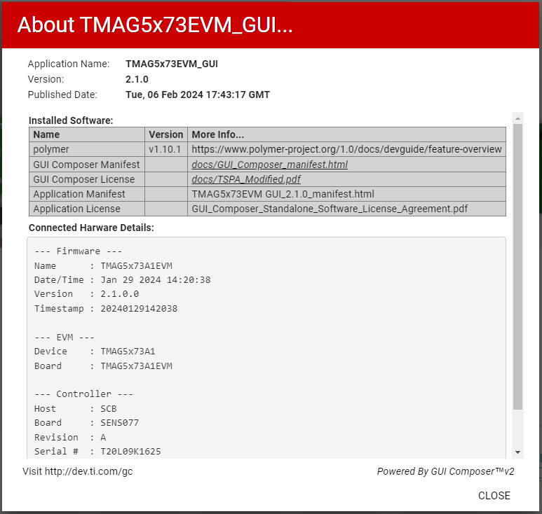
 - The date and time
obtained from this command is the same date and time that appears in the
GUI’s About screen (see Figure 4-21). Click the About option under the GUI's Help menu to
view the About screen.
 Figure 4-21 Firmware
Revision Version in GUI About Screen
- BSL command format: bsl
- This command puts the device in BSL mode, which is necessary before reflashing the SCB firmware. An alternative to entering BSL mode is to enter BSL mode in hardware as described in step 1b of Section 4.1.2.1. Before BSL is entered, LED D1 is on. If BSL mode is successfully entered, then LED D1 is turned off so that only the Power LED (LED D5) is on. After entering BSL mode, the device does not accept any of the above commands.
- Figure 4-22 shows an example response to this command:
 Figure 4-22 BSL Command
Response
Trigger conversion command format: rreg 0
- If the device is in standby mode and new conversions are set to be triggered through I2C, then doing a register read at register 0 automatically starts a new set of conversions.