SNAA291A May 2016 – April 2021 ADC32RF45 , LMX2582 , LMX2592
2 Understanding Phase Noise and Jitter and SNR
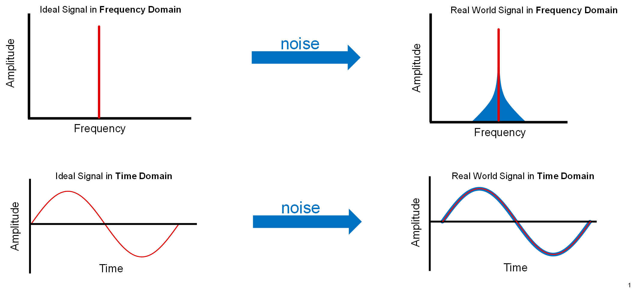
Designing for and finding out the lowest jitter starts from knowing the phase noise of a clock signal from a synthesizer. In the time domain, an ideal sine-wave clock signal looks like the waveform in the bottom-left of Figure 2-1. Realistically, due to the real world imperfections of components of a frequency synthesizer, there is additional noise which deviates the waveform from its ideal positions. Similarly, the same sine-wave converted to the frequency domain is a single pulse at the frequency of oscillation. The noise addition appears in the form of phase noise (skirts beside the ideal pulse). Low phase noise of a synthesizer suggests that the signal is cleaner, provides better performance, and ultimately has lower jitter (discussed in Section 3) to clock the ADC.
 Figure 2-1 Phase Noise in the Frequency and Time Domain
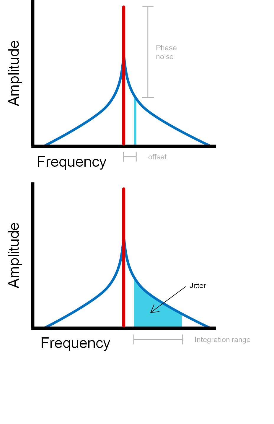
Phase noise is defined by the ratio of noise (at an offset frequency from the oscillating signal, with a 1-Hz bandwidth) to the signal amplitude of the oscillating signal. Integrated noise is essentially the sum of all the phase noise within a defined range of offset frequencies from the oscillating signal (see Figure 2-2). Jitter is derived from Equation 2 using the integrated noise and the frequency of the signal:

The integration range selected is important. This is determined by the sampling settings of the ADC. The bottom range (closer to the oscillating signal) is defined by half of [sampling rate] / [FFT size]. For example, at a sample rate of 2949.12 MHz and FFT size of 65536, the integration goes down to 22.5 kHz (see SLYT379 for more information). Thus, the lower this bottom of the integration range, the more the phase noise at lower offsets matter.
 Figure 2-2 Phase Noise and Jitter Definitions