SNAA343A March 2021 – May 2021 TPL5110-Q1
4 Pin Failure Mode Analysis (Pin FMA)
This section provides a Failure Mode Analysis (FMA) for the pins of the TPL5110-Q1. The failure modes covered in this document include the typical pin-by-pin failure scenarios:
- Pin short-circuited to Ground (see Table 4-2)
- Pin open-circuited (see Table 4-3)
- Pin short-circuited to an adjacent pin (see Table 4-4)
- Pin short-circuited to VDD (see Table 4-5)
Table 4-2 through Table 4-5 also indicate how these pin conditions can affect the device as per the failure effects classification in Table 4-1.
| Class | Failure Effects |
|---|---|
| A | Potential device damage that affects functionality |
| B | No device damage, but loss of functionality |
| C | No device damage, but performance degradation |
| D | No device damage, no impact to functionality or performance |
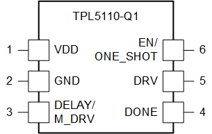
Figure 4-1 shows the TPL5110-Q1 pin diagram. For a detailed description of the device pins please refer to the Pin Configuration and Functions section in the TPL5110-Q1 data sheet.
 Figure 4-1 Pin Diagram
Following are the assumptions of use and the device configuration assumed for the pin FMA in this section:
- Device used within the Recommended Operating Ratings and the Absolute Maximum Ratings found in the TPL5110-Q1 data sheet.
- Configuration as a timer as shown in the Typical Application found in the TPL5110-Q1 data sheet.
| Pin Name | Pin No. | Description of Potential Failure Effect(s) | Failure Effect Class |
|---|---|---|---|
|
VDD |
1 |
Device may not power on. No current flow. |
B |
|
GND |
2 |
Typically tied to GND. |
D |
|
DELAY/M_DRV |
3 |
May default to minimum delay value of 100ms. |
C |
|
DONE |
4 |
DRV output forced to minimum duty cycle, remaining low TIP - 50ms, and returning high for 50ms. |
C |
|
DRV |
5 |
Output is forced low. |
B |
|
EN/ONE_SHOT |
6 |
Forces one-shot operation. |
C |
| Pin Name | Pin No. | Description of Potential Failure Effect(s) | Failure Effect Class |
|---|---|---|---|
|
VDD |
1 |
No functionality. |
B |
|
GND |
2 |
Device will not power on. No current flow. |
B |
|
DELAY/M_DRV |
3 |
Device may not complete initialization. May default to maximum time interval. |
B |
|
DONE |
4 |
DRV output will have minimum duty cycle, remaining low TIP - 50ms, and returning high for 50ms. |
C |
|
DRV |
5 |
No output. |
B |
|
EN/ONE_SHOT |
6 |
May operate in timer or one-shot mode. |
C |
| Pin Name | Pin No. | Shorted to | Description of Potential Failure Effect(s) | Failure Effect Class |
|---|---|---|---|---|
|
VDD |
1 |
GND |
Device may not power on. No current flow. |
B |
|
GND |
2 |
DELAY/M_DRV |
May force time interval to minimum. |
C |
|
DELAY/M_DRV |
3 |
DONE |
May force manual MOSFET power on. |
B |
|
DONE |
4 |
DRV |
DRV output will have minimum duty cycle, remaining low TIP - 50ms, and returning high for 50ms. |
C |
|
DRV |
5 |
EN/ONE_SHOT |
May operate in timer or one-shot mode. |
C |
|
EN/ONE_SHOT |
6 |
VDD |
Forces timer operation. |
C |
| Pin Name | Pin No. | Description of Potential Failure Effect(s) | Failure Effect Class |
|---|---|---|---|
|
VDD |
1 |
Typically tied to VDD. |
D |
|
GND |
2 |
Device may not power on. No current flow. |
B |
|
DELAY/MC_DRV |
3 |
Device may not complete initialization. DRV output may be forced low. |
B |
|
DONE |
4 |
Impacts DRV output pulse width for one period. |
C |
|
DRV |
5 |
Output is forced high. |
B |
|
EN/ONE_SHOT |
6 |
Forces timer operation. |
C |