SNAA361A april 2022 – may 2023 LMX2820
4.1 External VCO Loop Filter Design
The gain (kV) of the external VCO is significantly different than the internal VCO of the LMX2820. As such, the loop filter must be modified to achieve optimum performance. Use TI’s PLLatinum™ Simulation Software tool version 1.6.0 or later to optimize the loop filter for the external VCO.
Within the PLLatinum simulation GUI, select the LMX2820 from the Select Device menu. This will pre-load the standard configuration for the device. Adjust the following parameters to reflect the set-up configuration and external VCO parameters:
- Fosc, Fpfd: 375 MHz highest PFD frequency yields best phase noise
- Fout, FVCO: 9000 MHz set the VCO frequency to 9 GHz
- KVCO: 0.6 MHz/V VCO gain extracted from its data sheet
- Change Filter Designer > 3rd-order filter
- Select Active B topology
Also toggle the Advanced radial button under Feature Level. Within the Phase Noise tab, load a user-specified phase noise file reflecting the reference frequency of the system. This analysis uses a file derived from the measured performance of the SMA100B signal generator operating at 375 MHz. Next, load a file for the open loop phase noise of the external VCO (either from measurement or from the device data sheet). Table 4-1 shows the values used in this analysis.
| Frequency Offset (Hz) | Phase Noise (dBc/Hz) | Notes |
|---|---|---|
|
1000 |
-77.8 |
From data sheet |
|
10000 |
-106.2 |
From data sheet |
|
100000 |
-126.5 |
From data sheet |
|
10000000 |
-146 |
Measured |
|
20000000 |
-150 |
Measured |
|
40000000 |
-154 |
Measured |
|
100000000 |
-154 |
Measured |
In the Integrated Noise section, change the limits of integration as desired. For this analysis, the limits are 10 kHz to 40 MHz. Pushing the start frequency out to 10 kHz focuses more importance on the PLL and VCO performance and less on the reference frequency performance. For convenience, on the Filter Design tab in the Filter Optimizer section, select “Jitter (fs)” from the pull-down menu. This displays the simulated integrated jitter performance on the tab without having to switch to the Phase Noise tab to see the results.
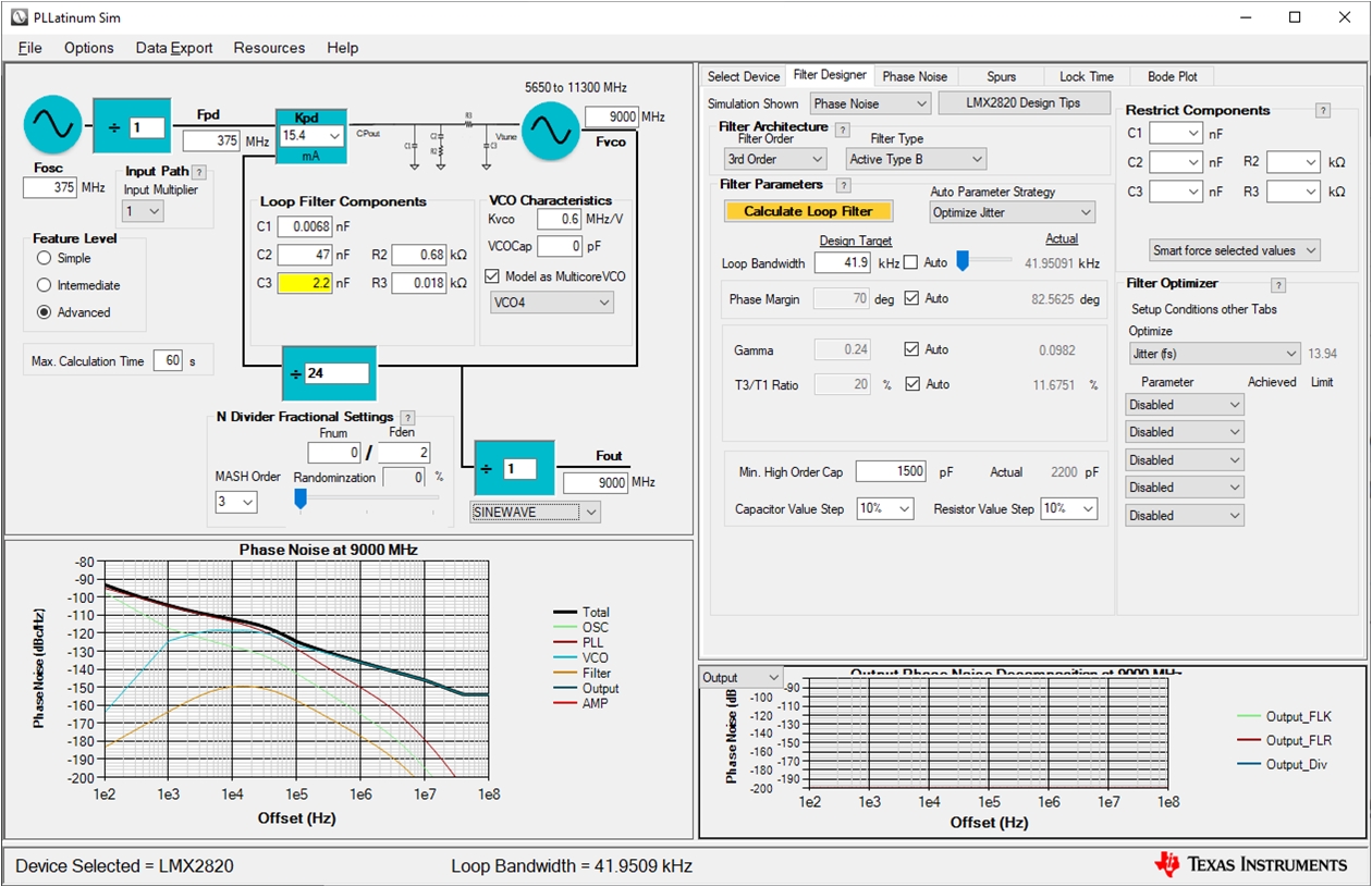
The active loop filter uses a 3rd-order topology corresponding to the Active B topology. The simulation tool graphs the composite phase noise performance along with the individual contributor components of the VCO and PLL. The default loop filter component values in the simulator will yield a peaky phase noise response once the previously-mentioned parameters are changed. This is primarily due to the very low VCO gain of the external VCO. Use the simulator to adjust loop filter values for the optimum response. The general strategy is to decrease the loop bandwidth of the filter to take advantage of the low VCO noise performance.
There are no absolute right values for the loop filter. There are a variety of combinations that will yield good results. The Calculate Loop Filter tool in the PLLatinum simulation tool assists with getting close to the goal. Adjust specific components to maintain minimum values or realizable values. From there, additional trial-and-error tweaks achieve optimal jitter performance.
For this analysis, the loop filter bandwidth is around 41 kHz. Figure 4-3 shows the simulation results. Disregard the warning related to the PFD frequency; anything less than 400 MHz is acceptable. Also disregard the warning on the capacitor value C1; keeping the value above 1.5 nF is preferable. Table 4-2 lists the loop filter component values for one optimized solution. The simulated RMS jitter from 10 kHz to 40 MHz is just under 14 fs.
 Figure 4-3 External VCO PLLatinum™
Simulation GUI Loop Filter
Figure 4-3 External VCO PLLatinum™
Simulation GUI Loop Filter| Simulation Reference Designator | Value |
|---|---|
|
C1 |
6.8 pF |
|
C2 |
47 nF |
|
R2 |
680 Ω |
|
C3 |
2.2 nF |
|
R3 |
18 Ω |