SNAA365 June   2024 LMK5B33216


  1.   1
  2.   Abstract
  3.   Trademarks
  4. 1Hardware Architecture
    1. 1.1 Clocking Scheme
    2. 1.2 FPGA Design
  5. 2syn1588® Synchronization Algorithm
    1. 2.1 PTP Time-of-Day Clock Adjustment Algorithm
  6. 3Test Setup
    1. 3.1 FMC Adapter Board
    2. 3.2 Compliance Test Setup
    3. 3.3 Compliance Test of Telecom Profile G.8275.1 - Full Timing Support
      1. 3.3.1 Transfer Characteristic
      2. 3.3.2 Absolute Time Error
      3. 3.3.3 Lock Time
    4. 3.4 Compliance Test of Telecom Profile G.8275.2 - Partial Timing Support
    5. 3.5 Compliance Test of Telecom Profile G.8262.1 - SyncE Transient
  7. 4PTP System Application
  8. 5Additional Development
  9. 6Conclusion
  10. 7References

Test Setup

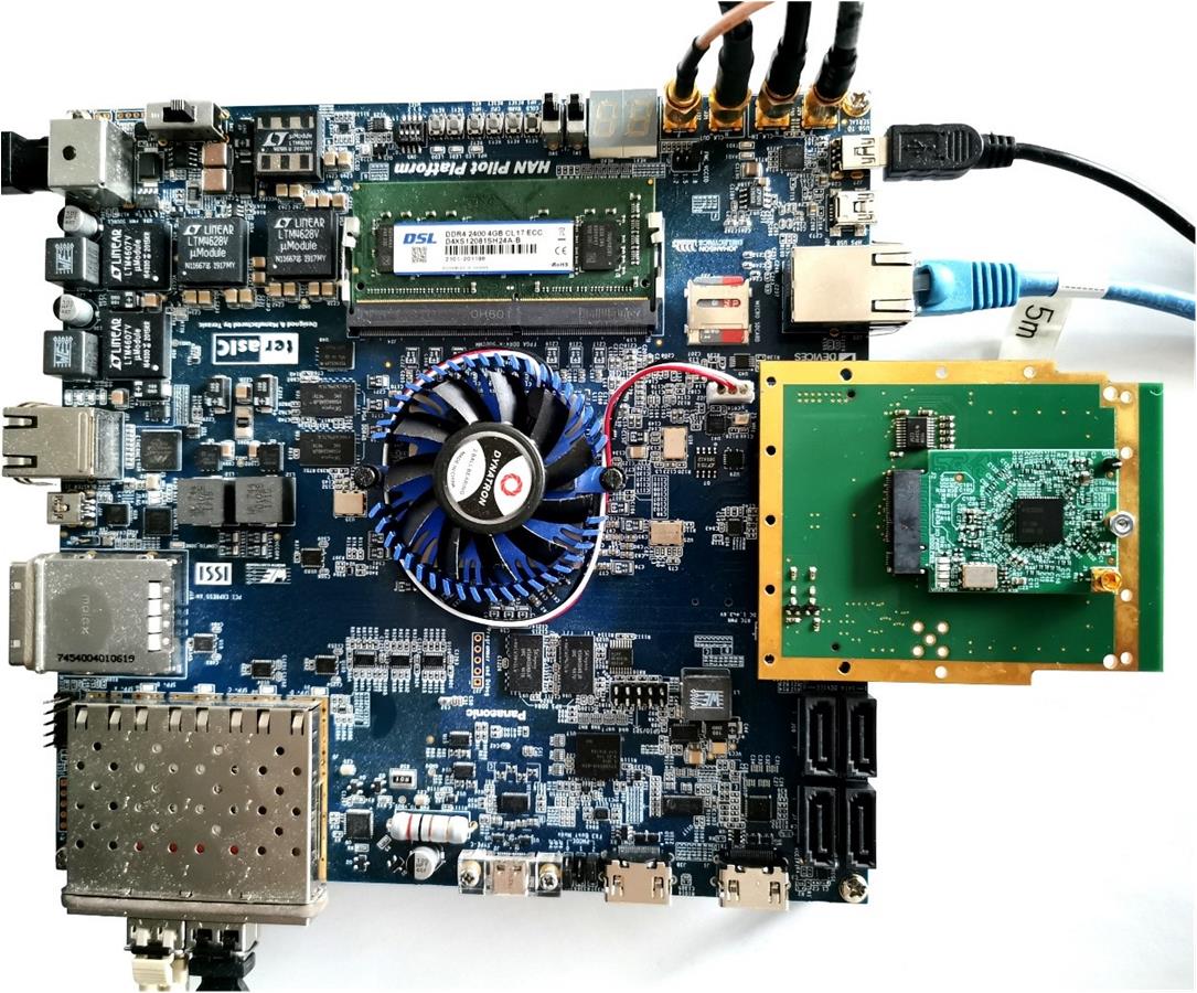
The PTP implementation on the Intel® FPGA is functionally tested by mounting the LMK5XXXXXS1 M2 module onto an interface connector board to match the FMC connector of the HAN Pilot platform. The setup is captured in Figure 3-1.
 Lab Measurement SetupFigure 3-1 Lab Measurement Setup