SNAA365 June 2024 LMK5B33216
- 1
- Abstract
- Trademarks
- 1Hardware Architecture
- 2syn1588® Synchronization Algorithm
- 3Test Setup
- 4PTP System Application
- 5Additional Development
- 6Conclusion
- 7References
3.1 FMC Adapter Board
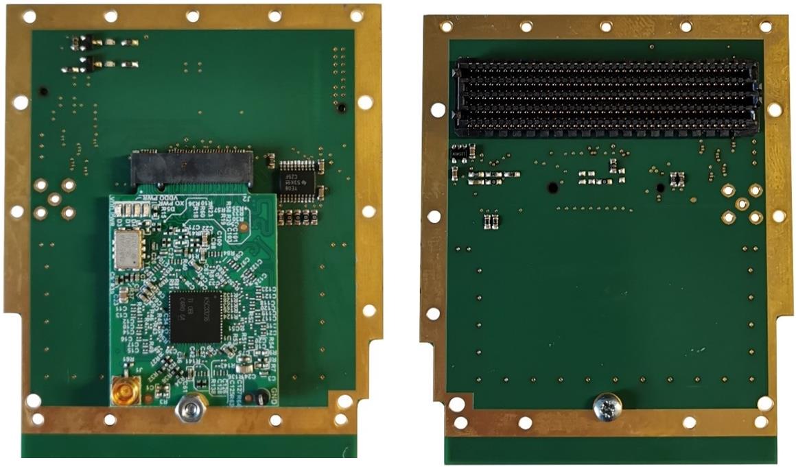
A dedicated FMC adapter board is designed to directly attach the LMK5XXXXXS1 M2 module to the HAN Pilot platform in parallel. The adapter board contains an M2 socket, a number of passive components (such as pull-up/pull-down resistors and AC-coupling capacitors), and several level shifters. The top and bottom side of the adapter board are shown in Figure 3-2.
 Figure 3-2 FMC Adapter Board Containing the LMK5XXXXXS1
M2 Module - Top (Left) and Bottom (Right)
Figure 3-2 FMC Adapter Board Containing the LMK5XXXXXS1
M2 Module - Top (Left) and Bottom (Right)In Figure 3-3, a connector schematic provides a more detailed view on the signals used from the LMK5XXXXXS1 M2 module, where REF0 (10MHz) is the primary input frequency for the network synchronizer. The secondary input, REF1 (156.25MHz), is the SyncE frequency extracted from the 10G Ethernet PHY port by the FPGA. OUT7 is the primary output frequency of the LMK5XXXXXS1, which is supplied directly to the PTP hardware clock. The value of the network timing PTP clock is adjusted by the PTP Stack as shown in Figure 1-3.
 Figure 3-3 FMC M2 Module Pins Used in FMC Adapter Board