SNAA401 April 2024 LMX2820
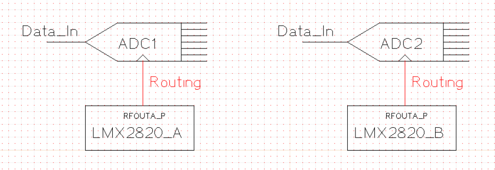
LMX2820 is RF synthesizer part, which can generate frequencies upto 22.6GHz at the output. This high frequency clock is used to clock ADC for sampling purpose. When clocking two ADCs from each of LMX2820, there could be some delay between sampling clock rising instants due to non-symmetrical routing. This non-zero delay between sampling clock rising instants can be adjusted using one of the two RF synthesizer MASH_SEED option. This option works till the maximum frequency of 22.6GHz. As showing in figure Figure 1, Clocks generated from LMX2820_A and LMX2820_B to ADC1 and ADC2 respectively might have some skew between rising edges due to non-symmetrical routing. Depending on the applications, clock frequency can go as high as 20GHz. So, adjusting clock skew to zero becomes critical.
 Figure 1 LMX2820 Clock Driving Two Independent ADCs
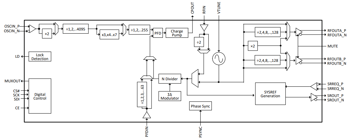
In general, PLLs are operated in fractional mode in multiple MASH orders namely first, second and third order. Functional block diagram of 2820 Synthesizer is shown in Figure 2.
 Figure 2 Functional Block Diagram
Delta-Sigma Modulator modulates the N Divider input based on the mash order used. Higher the mash order, higher the variation in clock periods coming out of N Divider. Following table shows the period variation at the output of N Divider. Ex: 0 means divide by N, 1 means divide by N+1. Seed means MASH_SEED(R41 and R42) and MASH_SEED_EN has to be made 1. Always program MASH_SEED to be less than Denominator. Consider an example where Numerator = 9 and Denominator = 21. So, Fraction is 0.428571429.
| 1st Order | 2nd Order | 3rd Order | |||||
|---|---|---|---|---|---|---|---|
| Clock Edge | 2820_A | 2820_B | 2820_A | 2820_B | 2820_A | 2820_B | |
| Seed = 0 for 2820_A and 0 for 2820_B | 1 | 0 | 0 | 0 | 0 | 0 | 0 |
| 2 | 0 | 0 | 0 | 0 | 0 | 0 | |
| 3 | 1 | 1 | 1 | 1 | 1 | 1 | |
| 4 | 0 | 0 | 0 | 0 | 0 | 0 | |
| 5 | 1 | 1 | 1 | 1 | 1 | 1 | |
| 6 | 0 | 0 | 0 | 0 | 0 | 0 | |
| 7 | 1 | 1 | 1 | 1 | 1 | 1 | |
| Seed = 3 for 2820_A Seed = 0 for 2820_B |
8 | 0 | 0 | 0 | 0 | 0 | 0 |
| 9 | 1 | 0 | 1 | 0 | 1 | 0 | |
| 10 | 0 | 1 | 1 | 1 | 1 | 1 | |
| 11 | 0 | 0 | -1 | 0 | 0 | 0 | |
| 12 | 1 | 1 | 2 | 1 | -1 | 1 | |
| 13 | 0 | 0 | -1 | 0 | 3 | 0 | |
| 14 | 1 | 1 | 1 | 1 | -2 | 1 | |
| 15 | 0 | 0 | 1 | 0 | 2 | 0 | |
| 16 | 1 | 0 | 0 | 0 | -1 | 0 | |
| 17 | 0 | 1 | 0 | 1 | 2 | 1 | |
| 18 | 0 | 0 | 1 | 0 | 0 | 0 | |
| 19 | 1 | 1 | 0 | 1 | 0 | 1 | |
| 20 | 0 | 0 | 0 | 0 | 1 | 0 | |
| 21 | 1 | 1 | 2 | 1 | 0 | 1 | |
| 22 | -1 | 0 | 0 | 0 | |||
| 23 | 1 | 0 | 1 | 0 | |||
| 24 | 0 | 1 | 0 | 1 | |||
| 25 | 1 | 0 | 1 | 0 | |||
| 26 | 0 | 1 | 1 | 1 | |||
| 27 | 1 | 0 | -1 | 0 | |||
| 28 | 0 | 1 | 1 | 1 | |||
Generalized formula for the delay when channel divider is not engaged(direct VCO) is as follows:
| Order | Delay in degrees of output Frequency |
|---|---|
| 1st Order | ( floor(SEED/GCD(NUM,DEN)) / (DEN/GCD(NUM,DEN) ) × 360 |
| 2nd Order and 3rd Order | (SEED/DEN × 360) |
Example:
- For 1st order , when MASH_SEED =1 and NUM/DEN = 9/21, there is not clock delay change addition. If MASH_SEED = 1 is written thrice, then delay between clocks of 2820_A and 2820_B is (1/7) × 360 degrees.
- For 2nd order and 3rd order, when MASH_SEED =1 and NUM/DEN =9/21, then delay between clocks of 2820_A and 2820_B is (1/21) × 360 degrees.
Remember that movement in Clock rising edge due to MASH_SEED depends on previous MASH_SEED written.