SNAA414 August 2024 LMX2820
Introduction
When using TI synthesizers, some common mistakes are easily mitigated. This application brief highlights some of the common mistakes to avoid so that users are efficiently able to set up the device. Topics that cover are as follows:
Clock synthesizer phase noise performance is bad and not as per data sheet specifications. What is going wrong?
How to simulate the performance of clock synthesizer with different Reference clock source phase noise?
Common issues with Input and Output terminations and impedance mismatches.
Impact of Slew rate of Reference on Clock Output Phase Noise
Impact of Clock Amplitude on ADC SNR performance
Clock synthesizer testing – debug flow
1. Phase noise performance of the clock synthesizer
A common mistake when using TI synthesizers is when the phase noise performance of the clock synthesizer does not match the data sheet specifications.
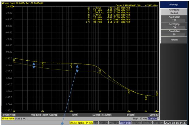 Figure 1 Phase noise performance of the clock synthesizer output with two different source
The difference in phase noise performance is not expected because both the light and bold traces in Figure 1 are from the same LMX2820 devices and set at the same 6GHZ output setting.
The bold trace in Figure 1 shows a degraded performance in comparison to the data sheet specification.
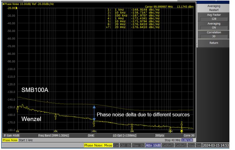 Figure 2 Different sources 100MHz Phase Noise Performance
The light trace in Figure 1 is generated with Wenzel 100MHz, used as a reference clock to the LMX2820 EVM. The degraded performance was generated using the SMB100A signal generator as a reference clock to the LMX2820 EVM.
In summary, the reference oscillator and source impacts the overall phase noise performance. To achieve performance data that is similar to the data sheet, use the good source as input to the LMX device.
Simulation of the LMX2820 with exact an source phase noise is available using the PLLatinum Sim software tool.
5052B Settings impact on phase noise
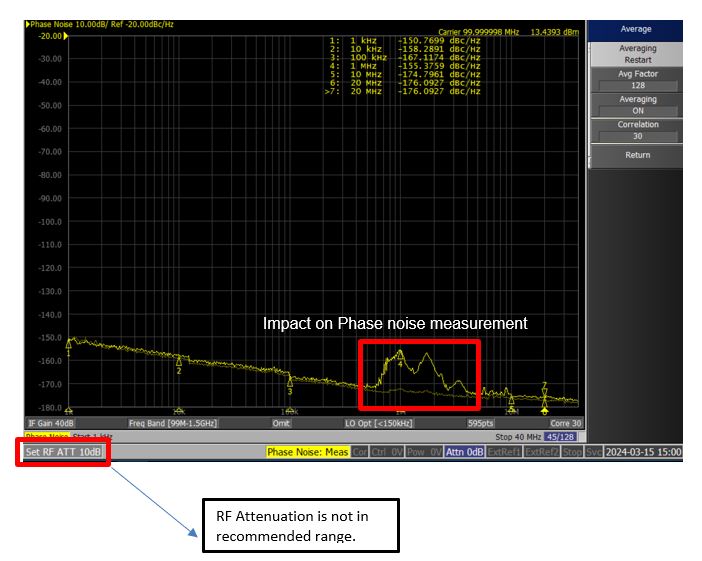 Figure 3 5052B Settings impact on phase noise
As shown in above in the Figure 3 graph, note warning settings before taking actual phase noise measurements. When checking the power on the PN analyzer, confirm that the trace loss on EVM is de-embedded, to calculate the power at the pin of the device.
2. Simulating the performance of a clock synthesizer with different phase noise of the reference clock source
 Figure 4 Clock Synthesizer Performance Simulation
Figure 4 shows the PLLatinum sim tool simulation window. Confirm that the settings on board are entered into PLLatinum and the phase margin is verified before checking PN plots.
Following Figure 5, Figure 6 shows the PLLatinum sim tool simulation results for two different input clock profiles.
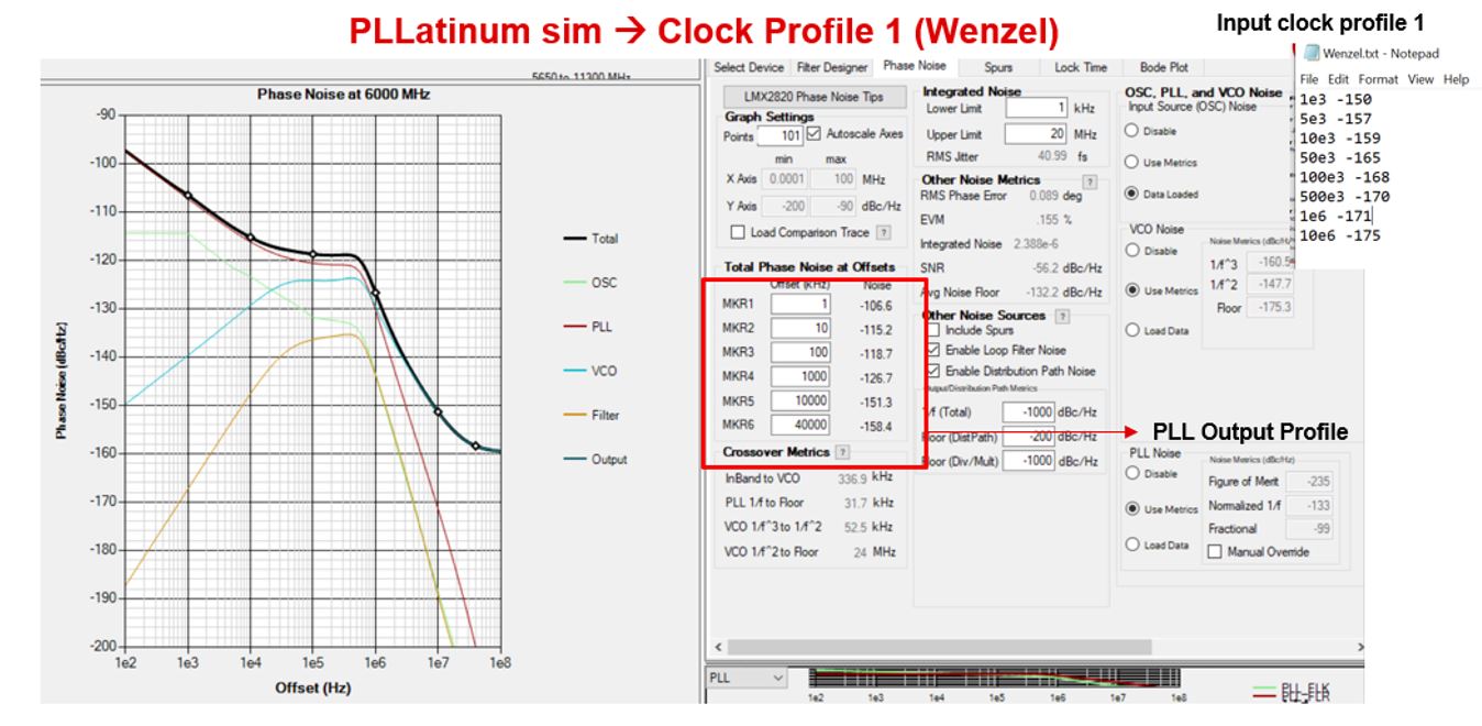 Figure 5 Output phase noise profile of LMX2820 with input Clock Profile 1 (Wenzel)
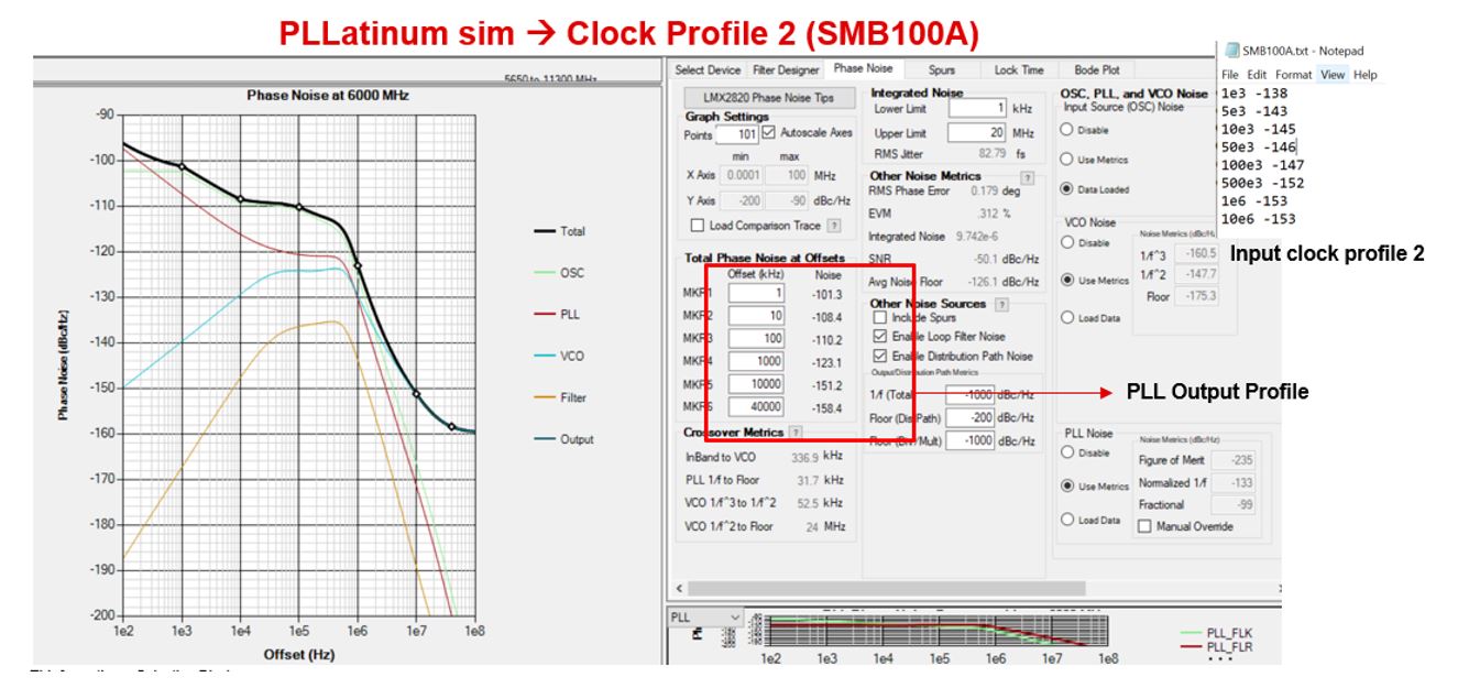 Figure 6 Output phase noise profile of LMX2820 with input Clock Profile 2 (SMB100A)
3. Common Issues with Input and Output terminations and Impedance Mismatches
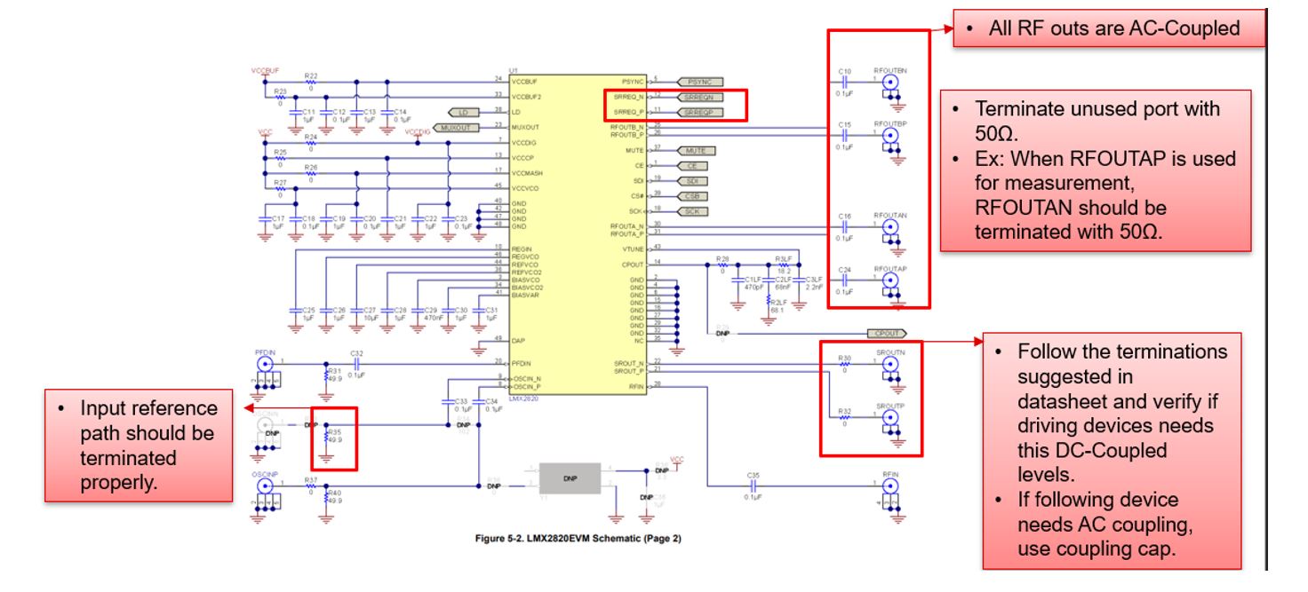 Figure 7 Common Issues with Input and Output terminations and Impedance Mismatches
Figure 7 shows various termination requirements based on input or output ports. Sometimes, there is damaged input coupling capacitor, which may damage the internal common mode operation for the input OSCIN_P pins and there could be issues with loop locking. Check to make sure the common mode at the OSCIN_P and OSCIN_N are the same.
4. Impact of Slew rate of Reference on Clock Output Phase Noise
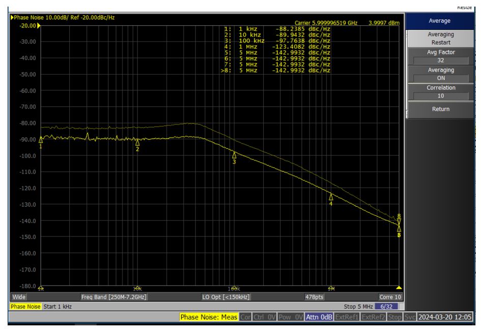 Figure 8 6GHz output on LMX2820 with reference (OSCIN) levels of -5dbm and 10dbm
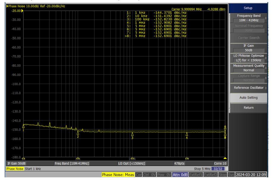 Figure 9 Reference (OSCIN) 10MHz reference PN plot for -5dbm and 10dbm
In general, low reference frequencies have less slew rate. At 10-MHz input, slew rate is very problematic. At 100-MHz input, there is 10 times the slew rate for the same power level. Even though there is minimal phase noise change at the input 10-MHz clock source for two different amplitude as shown in Figure 9, there is huge change in output phase noise as shown in Figure 8. Use a low noise buffers LMK1C1102 in the path of the 10MHz to boast the amplitude before giving to OSCIN_P.
5. Impact of clock amplitude on ADC SNR performance
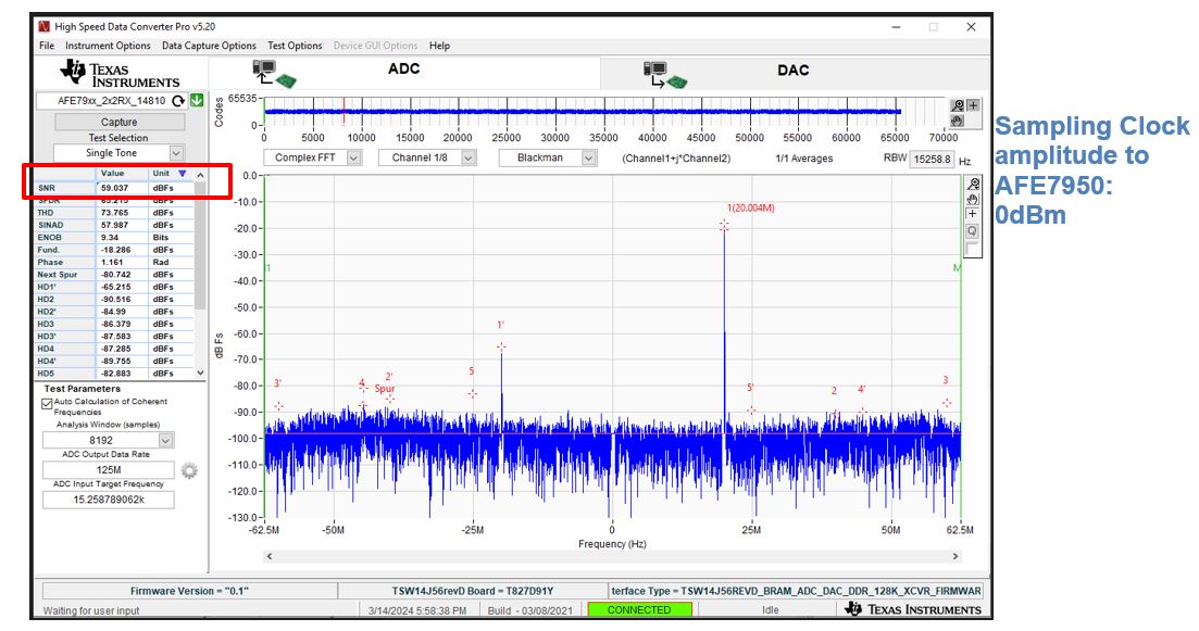 Figure 10 ADC capture with Sampling clock amplitude to AFE7950: 0dBm
AFE7950 FFT plot - 12GHz Sampling Clock (Fs) from LMX2820; Ain: -18dBFs. Input Frequency: 9520MHz; ADC Fs: 3GSPS; NCO: 9500MHz; Decimation:24
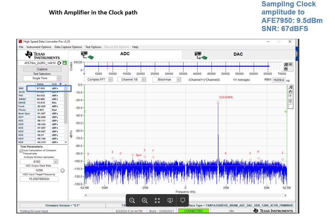 Figure 11 ADC capture with Sampling clock amplitude to AFE7950: 9.5Bm
AFE7950 FFT plot - 12GHz Sampling Clock (Fs) from LMX2820 + Amplifier (ZJL-153+) Input Frequency: 9520MHz; ADC Fs: 3GSPS; NCO: 9500MHz; Decimation:24
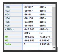 Figure 12 More Metrics from ADC capture
| Sampling clock from LMX2820 with different power levels | Sampling clock from LMC2820 and Amplifier (ZJL-153+) | Internal Clock (SNR) |
|---|---|---|
| 0.18dBm/59dBFs | 9.5dBm/67dBFs | 61.4dBFs |
| -1.91dBm/56dBFs | ||
| -3.19dBm/53dBFs | ||
| -4.86dBm/36dBFs |
For the best SNR performance, use an external clock with the highest amplitude recommended for the ADC.
When these features are together, there is a 4 - 5dB signal power loss due to many losses in the path of the signal:
- LMX2820 EVM output trace
- SMA
- AFE EVM SMA
- AFE EVM Balun
It is important to understand LMX2820 data sheet specification for power level and compare with the requirement for AFE ADC/DAC Clock power level, as shown in Table 1.
6. Clock synthesizer testing the debug flow
Figure 13 outlines the systematic debug of the PLL.
 Figure 13 Systematic Debug Flowchart
References
- Texas Instruments, A Survival Guide to Scaling Your PLL Loop Filter Design, technical article
- Texas Instruments, Timing Is Everything: Improving Integer Boundary Spurs in Fractional PLL Synthesizers, technical article