SNAS395F December 2007 – October 2016 DAC121C081 , DAC121C085
PRODUCTION DATA.
- 1 Features
- 2 Applications
- 3 Description
- 4 Revision History
- 5 Description (continued)
- 6 Pin Configuration and Functions
- 7 Specifications
- 8 Detailed Description
- 9 Application and Implementation
- 10Power Supply Recommendations
- 11Layout
- 12Device and Documentation Support
- 13Mechanical, Packaging, and Orderable Information
10 Power Supply Recommendations
10.1 Using References as Power Supplies
While the simplicity of the DAC121C081 implies ease of use, it is important to recognize that the path from the reference input (VA for the DAC121C081 and VREF for the DAC121C085) to VOUT will have essentially zero Power Supply Rejection Ratio (PSRR). Therefore, it is necessary to provide a noise-free supply voltage to the reference. To use the full dynamic range of the DAC121C085, the supply pin (VA) and VREF can be connected together and share the same supply voltage. Because the DAC121C081 consumes very little power, a reference source may be used as the supply voltage. The advantages of using a reference source over a voltage regulator are accuracy and stability. Some low noise regulators can also be used. Listed below are a few reference and power supply options for the DAC121C081. When using the DAC121C081, it is important to treat the analog supply (VA) as the reference.
10.1.1 LM4132
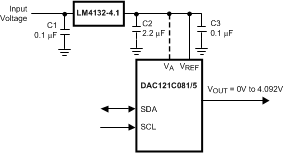
The LM4132, with its 0.05% accuracy over temperature, is a good choice as a reference source for the DAC121C081. The 4.096-V version is useful if a 0-V to 4.095-V output range is desirable or acceptable. Bypassing the LM4132 VIN pin with a 0.1-µF capacitor and the VOUT pin with a 2.2-µF capacitor improves stability and reduces output noise. The LM4132 comes in a space-saving 5-pin SOT-23.
 Figure 31. The LM4132 as a Power Supply
10.1.2 LM4050
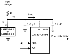
Available with accuracy of 0.44%, the LM4050 shunt reference is also a good choice as a reference for the DAC121C081. It is available in 4.096-V and 5-V versions and comes in a space-saving, 3-pin SOT-23.
 Figure 32. The LM4050 as a Power Supply
The minimum resistor value in the circuit of Figure 32 must be chosen such that the maximum current through the LM4050 does not exceed its 15-mA rating. The conditions for maximum current include the input voltage at its maximum, the LM4050 voltage at its minimum, and the DAC121C081 drawing zero current. The maximum resistor value must allow the LM4050 to draw more than its minimum current for regulation plus the maximum DAC121C081 current in full operation. The conditions for minimum current include the input voltage at its minimum, the LM4050 voltage at its maximum, the resistor value at its maximum due to tolerance, and the DAC121C081 draws its maximum current. These conditions can be summarized as
where
- VZ(min) is the nominal LM4050 output voltage ± the LM4050 output tolerance over temperature.
- IZ(max) is the maximum allowable current through the LM4050.
and
where
- VZ(max) is the nominal LM4050 output voltage ± the LM4050 output tolerance over temperature.
- IDAC(max) is the maximum DAC121C081 supply current.
- IZ(min) is the minimum current required by the LM4050 for proper regulation.
10.1.3 LP3985
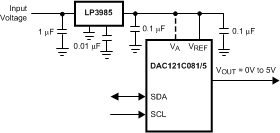
The LP3985 is a low noise, ultra low dropout voltage regulator with a 3% accuracy over temperature. It is a good choice for applications that do not require a precision reference for the DAC121C081. It comes in 3-V, 3.3-V and 5-V versions, among others, and sports a low 30-µV noise specification at low frequencies. Because low-frequency noise is relatively difficult to filter, this specification could be important for some applications. The LP3985 comes in a space-saving 5-pin SOT-23 and 5-bump DSBGA packages.
 Figure 33. Using the LP3985 Regulator
An input capacitance of 1 µF without any ESR requirement is required at the LP3985 input, while a 1-µF ceramic capacitor with an ESR requirement of 5 mΩ to 500 mΩ is required at the output. Careful interpretation and understanding of the capacitor specification is required to ensure correct device operation.
10.1.4 LP2980
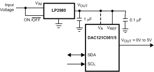
The LP2980 is an ultra low dropout regulator with a 0.5% or 1% accuracy over temperature, depending upon grade. It is available in 3-V, 3.3-V, and 5-V versions, among others.
 Figure 34. Using the LP2980 Regulator
Like any low dropout regulator, the LP2980 requires an output capacitor for loop stability. This output capacitor must be at least 1-µF over temperature, but values of 2.2 µF or more will provide even better performance. The ESR of this capacitor should be within the range specified in the LP2980 (SNOS733) data sheet. Surface-mount solid tantalum capacitors offer a good combination of small size and ESR. Ceramic capacitors are attractive due to their small size but generally have ESR values that are too low for use with the LP2980. Aluminum electrolytic capacitors are typically not a good choice due to their large size and have ESR values that may be too high at low temperatures.