SNAS407H August 2007 – April 2015 DAC128S085
PRODUCTION DATA.
- 1 Features
- 2 Applications
- 3 Description
- 4 Revision History
- 5 Description (continued)
- 6 Pin Configuration and Functions
- 7 Specifications
- 8 Detailed Description
- 9 Application and Implementation
- 10Power Supply Recommendations
- 11Layout
- 12Device and Documentation Support
- 13Mechanical, Packaging, and Orderable Information
9 Application and Implementation
NOTE
Information in the following applications sections is not part of the TI component specification, and TI does not warrant its accuracy or completeness. TI’s customers are responsible for determining suitability of components for their purposes. Customers should validate and test their design implementation to confirm system functionality.
9.1 Application Information
9.1.1 Using References as Power Supplies
While the simplicity of the DAC128S085 implies ease of use, it is important to recognize that the path from the reference input (VREF1,2) to the DAC outputs has a zero Power Supply Rejection Ratio (PSRR). Therefore, the user must provide a noise-free supply voltage to VREF1,2. To utilize the full dynamic range of the DAC128S085, the supply pin (VA) and VREF1,2 can be connected together and share the same supply voltage. Because the DAC128S085 consumes very little power, a reference source can be used as the reference input or the supply voltage. The advantages of using a reference source over a voltage regulator are accuracy and stability. Some low-noise regulators can also be used. Listed below are a few reference and power supply options for the DAC128S085.
9.2 Typical Application
The LM4132, with its ±0.05% accuracy over temperature, is a good choice as a reference source for the DAC128S085. The 4.096-V version is useful for a 0-V to 4.095-V output range. Bypassing the LM4132 voltage input pin with a 4.7-µF capacitor and the voltage output pin with a 4.7-µF capacitor improves stability and reduces output noise. The LM4132 comes in a space-saving 5-pin SOT-23.
 Figure 32. The LM4132 as a Power Supply
9.2.1 Design Requirements
There are two references for the DAC128S085. One reference input serves channels A through D, while the other reference serves channels E through H. The 16-bit input shift register of the DAC128S085 controls the mode of operation, the power-down condition, and the register/output value of the DAC channels. All eight DAC outputs can be updated simultaneously or individually.
9.2.2 Detailed Design Procedure
Each reference input pin can be set independently, or the reference pins can be shorted together as shown in Figure 32. Acceptable reference voltages are 0.5 V to VA. Utilizing an RC filter on the output to roll off output noise is optional.
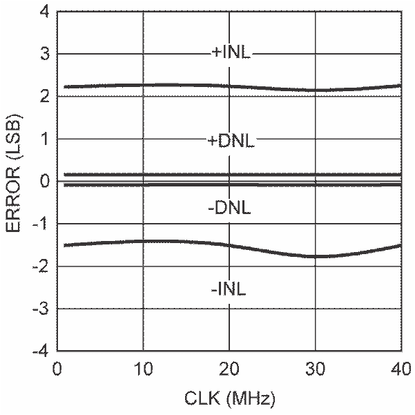
9.2.3 Application Curve
 Figure 33. Typical Performance