SNAS648C October 2014 – February 2023 TDC1000
PRODUCTION DATA
- 1 Features
- 2 Applications
- 3 Description
- 4 Revision History
- 5 Pin Configuration and Functions
- 6 Specifications
- 7 Parameter Measurement Information
-
8 Detailed Description
- 8.1 Overview
- 8.2 Functional Block Diagram
- 8.3 Feature Description
- 8.4 Device Functional Modes
- 8.5 Programming
- 8.6 Register Maps
- 9 Application and Implementation
- 10Device and Documentation Support
- 11Mechanical, Packaging, and Orderable Information
8.4.5.1 Timing Control and Frequency Scaling (CLKIN)
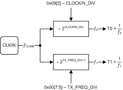
 Figure 8-22 External Clock Division Tree
All transmit and receive function sequencing is synchronous to the external clock applied to the CLKIN pin. The external clock is divided to generate two internal clocks with corresponding time periods denoted as T0 and T1 in #SNAS6484480. The division factor used to generate T0 is controlled with the CLOCKIN_DIV bit in the CLOCK_RATE register. The division factor used to generate T1 is controlled with the TX_FREQ_DIV field located in the CONFIG_0 register.
The SPI block is synchronous with the clock applied to the SCLK pin, and the block is independent of the clock applied to CLKIN. See the GUID-1E806E55-5183-4CD5-8A93-FE387C1817C6.html#TITLE-SNAS648SNAS6483438 section for a complete description of the SPI block.